Low temperature CVD process with selected stress of the CVD layer on CMOS devices

a cmos device and cvd layer technology, applied in the direction of mechanical equipment, manufacturing tools, rod connections, etc., can solve the problems of only achieving the required cvd reaction energy, pecvd process is unsuitable for fabricating 65 nanometer devices, and both processes may not be unsuitable for cvd processes for certain

Inactive Publication Date: 2007-09-13
APPLIED MATERIALS INC
View PDF99 Cites 263 Cited by
  • Summary
  • Abstract
  • Description
  • Claims
  • Application Information

AI Technical Summary

Benefits of technology

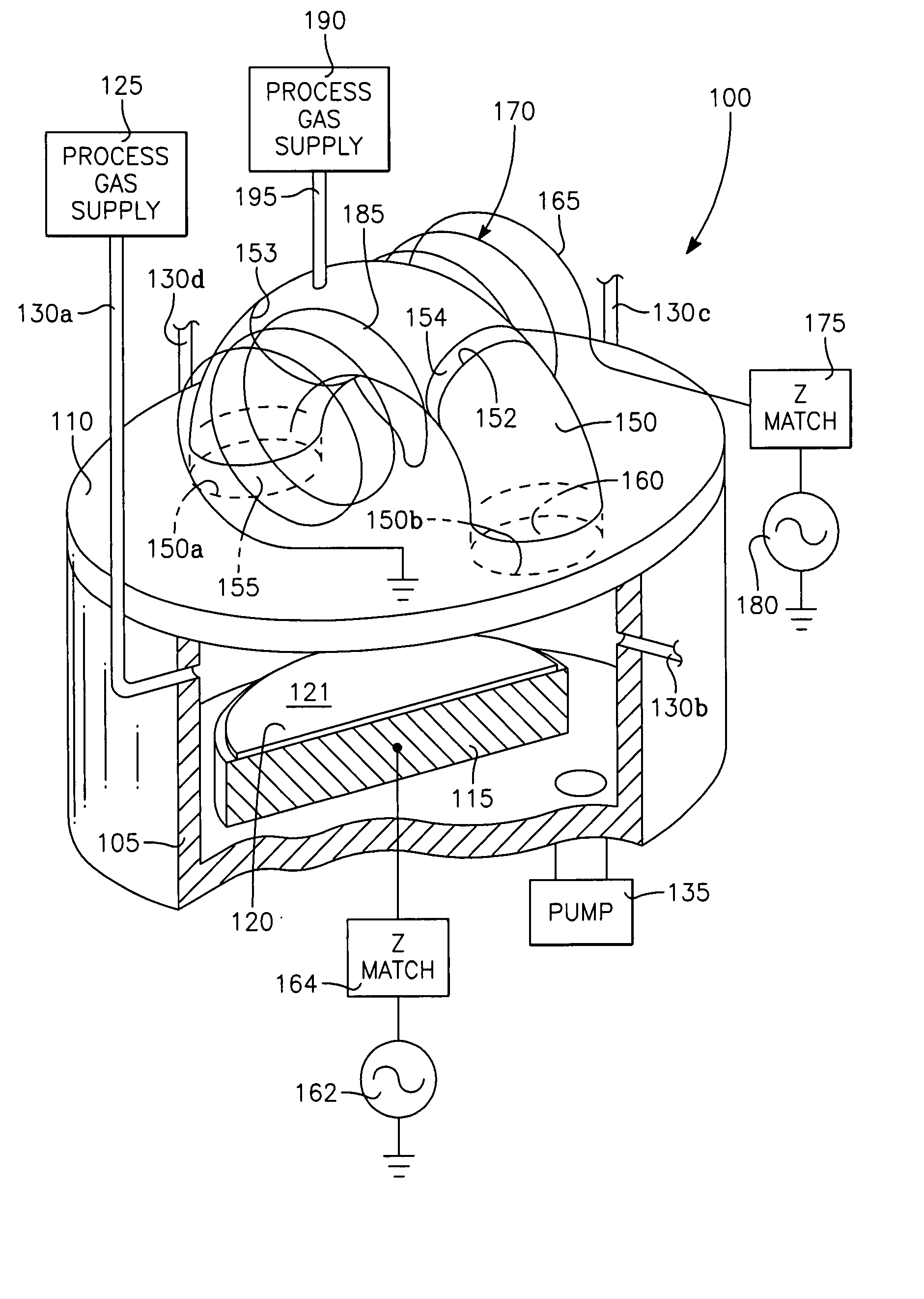
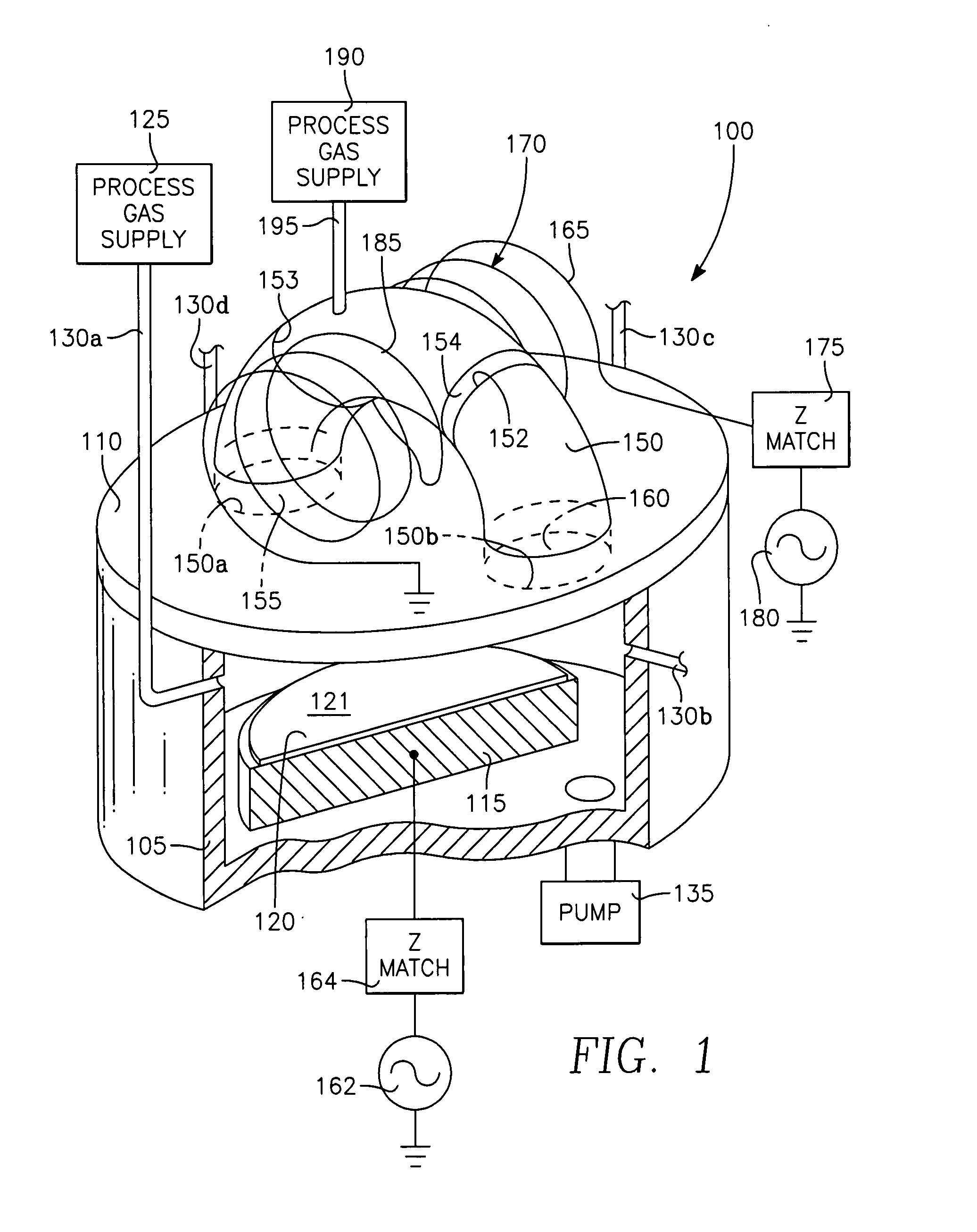
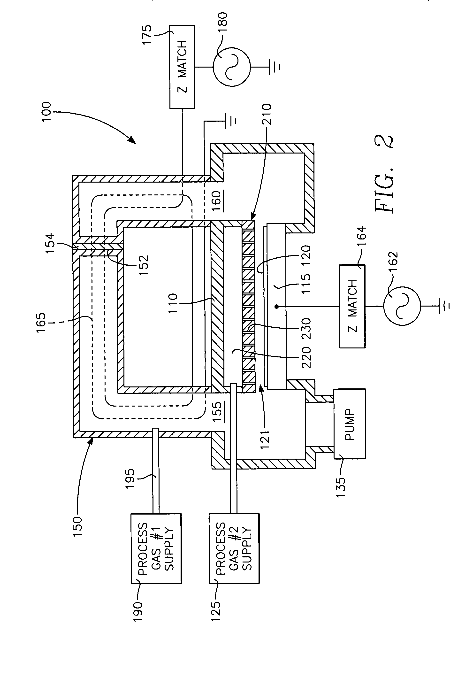
[0150] A further advantage of the invention is that because the RF inductive field is applied along the entire torroidal path of the RF plasma current (so that its absorption is distributed as discussed above), the chamber ceiling 110, unlike with most other inductively powered reactors, need not function as a window to an inductive field and therefore may be formed of any desired material, such as a highly conductive and thick metal, and therefore may comprise a conductive gas distribution plate as will be described below, for example. As a result, the ceiling 110 readily provides a reliable electric potential or ground reference across the entire plane of the pedestal or wafer 120.

Problems solved by technology

Both of these process may not be unsuitable for CVD processes for certain emerging integrated circuit technologies, specifically for the 65 nanometer technology at which features sizes are on the order of nanometers.
The PECVD process is unsuitable for fabricating 65 nanometer devices because the high chamber pressure employed by this process to boost the CVD deposition rate produces a high ion recombination rate, so that the plasma ion density is relatively small (about 10−5 ions / cc).
Therefore, the required CVD reaction energy can only be attained by heating the wafer to a relatively high temperature to supply the required chemical energy thermodynamically.
Furthermore, the high chamber pressure results in such a high CVD deposition rate that the deposited film has a flake-like structure unless the wafer is heated to about 400° C. This has the effect of annealing out the flake-like imperfection in the crystal growth during deposition.
A problem arises in using such a PECVD process to fabricate 65 nm wafers.
Reducing the wafer temperature to avoid diffusion beyond the 65 nm critical distance results in an unacceptably poor film quality.
Therefore, the PECVD process employing a high chamber pressure is unsuitable for depositing high quality films on 65 nm devices.
Such an inductively coupled reactor operated at such a low chamber pressure and low frequency cannot strike or maintain plasma without the application of a relatively large amount of source power, namely about 2 kW (minimum) of source power.
This creates a problem, in that the minimum plasma ion density produces excessive plasma-heating of the wafer, driving the wafer temperature to about 400° C. Since this occurs at the minimum source power of the reactor for plasma ignition or plasma maintenance, the wafer temperature in the HDPCVD reactor is necessarily too high for a 65 nm device.
Another disadvantage of the PECVD and HDPCVD processes is independent of the device feature size, and arises from the high wafer temperatures that are required in the PECVD process and are unavoidable in the HDPCVD process: photoresist masking cannot survive such processes because the high wafer temperatures exceed the temperature at which photoresist is destroyed or removed from the wafer.
Therefore, these PECVD and HDPCVD processes can only be employed in process steps requiring no photoresist masking, which greatly limits the utility of chemical vapor deposition (CVD) processes generally.
This is not feasible because the HDPCVD process relies on a very high plasma ion density to furnish the required energy to carry out the CVD growth or deposition reaction.
This forces a high degree of conformality in the HDPCVD-deposited layer which cannot be escaped.
However, this has not been generally regarded as a problem because such processes have not been viewed as vehicles for adjusting conformality between high conformality and non-conformality.
Another problem with conventional CVD processes arises in the filling of high aspect-ratio openings such as deep or shallow isolation trenches.
The problem is that sidewall deposition during a CVD process for filling such a trench pinches off the bottom of the trench before it is filled, leaving an impermissible void in the completed structure.
This practice, however, limits the processes that can be used for trench filling.

Method used


Image

  • Low temperature CVD process with selected stress of the CVD layer on CMOS devices
  • Low temperature CVD process with selected stress of the CVD layer on CMOS devices
  • Low temperature CVD process with selected stress of the CVD layer on CMOS devices

Examples


working examples

[0318] A principal application of a PIII reactor is the formation of PN junctions in semiconductor crystals. FIGS. 109 and 110 illustrate different stages in the deposition of dopant impurities in the fabrication of a P-channel metal oxide semiconductor field effect transistor (MOSFET). Referring first to FIG. 109, a region 9960 of a semiconductor (e.g., silicon) wafer may be doped with an N-type conductivity impurity, such as arsenic or phosphorus, the region 9960 being labeled “n” in the drawing of FIG. 109 to denote its conductivity type. A very thin silicon dioxide layer 9962 is deposited on the surface of the wafer including over n-type region 9960. A polycrystalline silicon gate 9964 is formed over the thin oxide layer 9962 from a blanket polysilicon layer that has been doped with boron in the PIII reactor. After formation of the gate 9964, p-type dopant is implanted in the PIII reactor to form source and drain extensions 9972 and 9973. Spacer layers 9966 of a dielectric mater...


PUM

PropertyMeasurementUnit
sizesaaaaaaaaaa
temperatureaaaaaaaaaa
critical distanceaaaaaaaaaa

Abstract

Device-enhancing coatings are deposited on CMOS devices by successively masking with photoresist each one of the sets of N-channel and P-channel devices while unmasking or leaving unmasked the other set, and after each step of successively masking one of the sets of devices, carrying out low temperature CVD steps with a toroidal RF plasma current while applying an RF plasma bias voltage. The temperature of the workpiece is held below a threshold photoresist removal temperature. The RF bias voltage is held at a level at which the coating is deposited with a first stress when the unmasked set consists of the P-channel devices and with a second stress when the unmasked set consists of N-channel devices.

Description

CROSS-REFERENCE TO RELATED APPLICATIONS [0001] This application is a divisional of U.S. patent application Ser. No. 10 / 838,052 filed May 30, 2004 entitled VERY LOW TEMPERATURE CVD PROCESS WITH INDEPENDENTLY VARIABLE CONFORMALITY, STRESS AND COMPOSITION OF THE CVD LAYER by Hiroji Hanawa et al., which is a continuation-in-part of U.S. Pat. No. 6,893,907 issued May 17, 2005 entitled FABRICATION OF SILICON-ON-INSULATOR STRUCTURE USING PLASMA IMMERSION ION IMPLANTATION by Dan Maydan et al., which is a continuation-in-part of co-pending U.S. patent application Ser. No. 10 / 646,533 filed Aug. 22, 2003 entitled PLASMA IMMERSION ION IMPLANTATION PROCESS USING A PLASMA SOURCE HAVING LOW DISSOCIATION AND LOW MINIMUM PLASMA VOLTAGE by Kenneth Collins et al., which is a continuation-in-part of U.S. Pat. No. 6,939,434 issued Sep. 6, 2005 entitled EXTERNALLY EXCITED TORROIDAL PLASMA SOURCE WITH MAGNETIC CONTROL OF ION DISTRIBUTION by Kenneth Collins et al. [0002] The following applications contain ...

Claims


Application Information

Patent Timeline
Patent Type & Authority Applications(United States)
IPC IPC(8): H01L21/16C23C14/48C23C16/507H01J37/32H01L21/223H01L21/265H01L21/316H01L21/318H01L21/336H01L21/8238
CPCC23C14/48Y10T29/5313H01J37/321H01J37/32174H01J37/32357H01J37/32412H01J2237/2001H01L21/2236H01L21/26513H01L21/31604H01L21/318H01L21/823807H01L21/823814H01L21/823842H01L29/6659C23C16/507H01L21/2658H01L21/02274H01L21/02126E04C5/165F16B7/0406
Inventor HANAWA, HIROJIRAMASWAMY, KARTIKCOLLINS, KENNETH S.AL-BAYATI, AMIRGALLO, BIAGIONGUYEN, ANDREW
Owner APPLIED MATERIALS INC
Why Eureka
Try Eureka