

Polishing composition for semiconductor wafer, production method thereof, and polishing method
a technology of polishing composition and semiconductor wafer, which is applied in the direction of manufacturing tools, other chemical processes, chemistry apparatus and processes, etc., can solve the problems of affecting the yield and quality of products, abrasive particles remain on the wafer surface, and the polishing speed is largely lowered
- Summary
- Abstract
- Description
- Claims
- Application Information
AI Technical Summary
Benefits of technology
Problems solved by technology
Method used
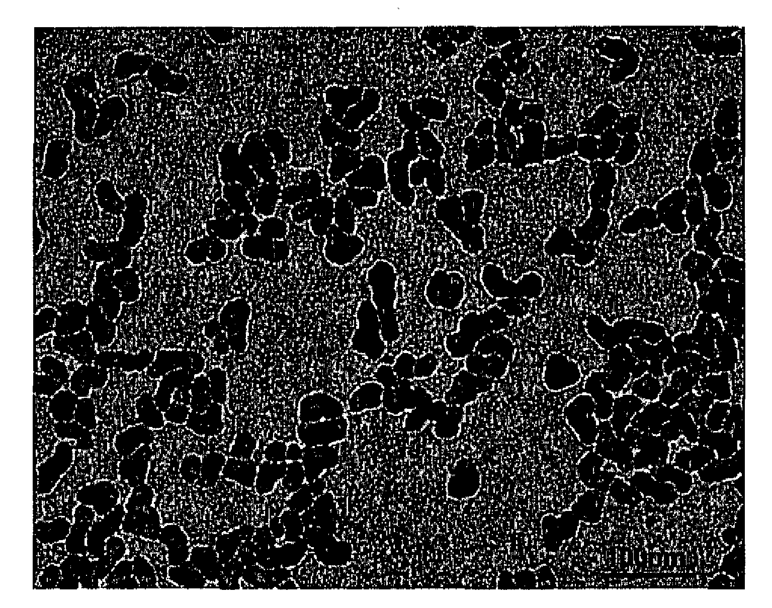
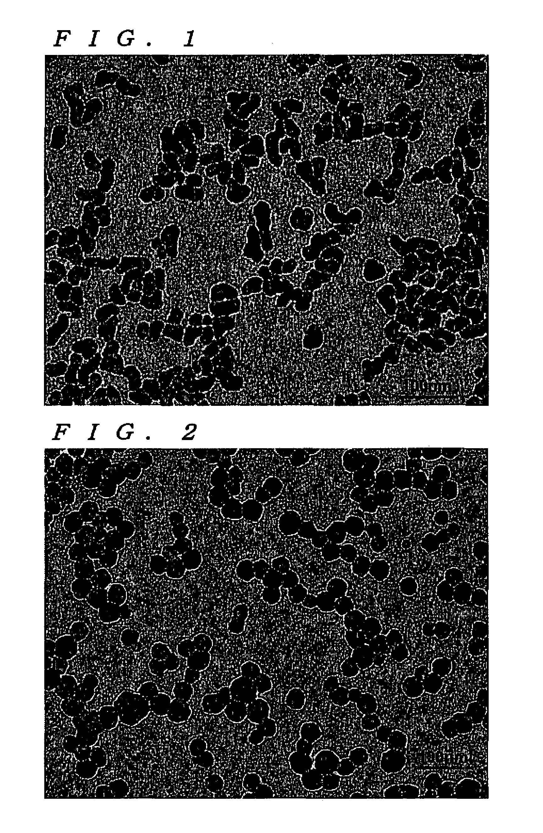
Image

Examples
example
(1) Production Example of Colloidal Silica Raw Material-A
[0065]A dilute soda-silicate having a silica concentrated of 4.5 wt % was prepared by adding 520 kg of JIS No. 3 soda-silicate (SiO2: 28.8 wt %, Na2O: 9.7 wt %, H2O: 61.5 wt %) to 2810 kg of deionized water and uniformly mixing them. The dilute soda-silicate was dealkalized by passing it through a 1,000-liter column of a H-type strong acid cation exchange resin (AMBERLITE IR120B manufactured by ORGANO Corp.) that was preliminary regenerated with hydrochloric acid. In this way, 3800 kg of an active silicic acid having a pH of 2.9 and a silica concentration of 3.7 wt % were obtained. The Na and K contents based on silica in the active silicic acid were 80 ppm and 5 ppm, respectively. After that, colloid particles were grown by the build-up process. To the part (580 kg) of the active silicic acid thus obtained, a 20 wt % tetramethylammonium hydroxide aqueous solution was added with stirring to adjust the pH at 8.7, and then the m...
PUM
| Property | Measurement | Unit |
|---|---|---|
| Temperature | aaaaa | aaaaa |
| Percent by mass | aaaaa | aaaaa |
| Electrical conductivity | aaaaa | aaaaa |
Abstract
Description
Claims
Application Information