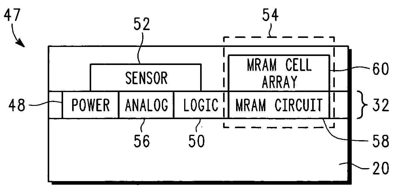
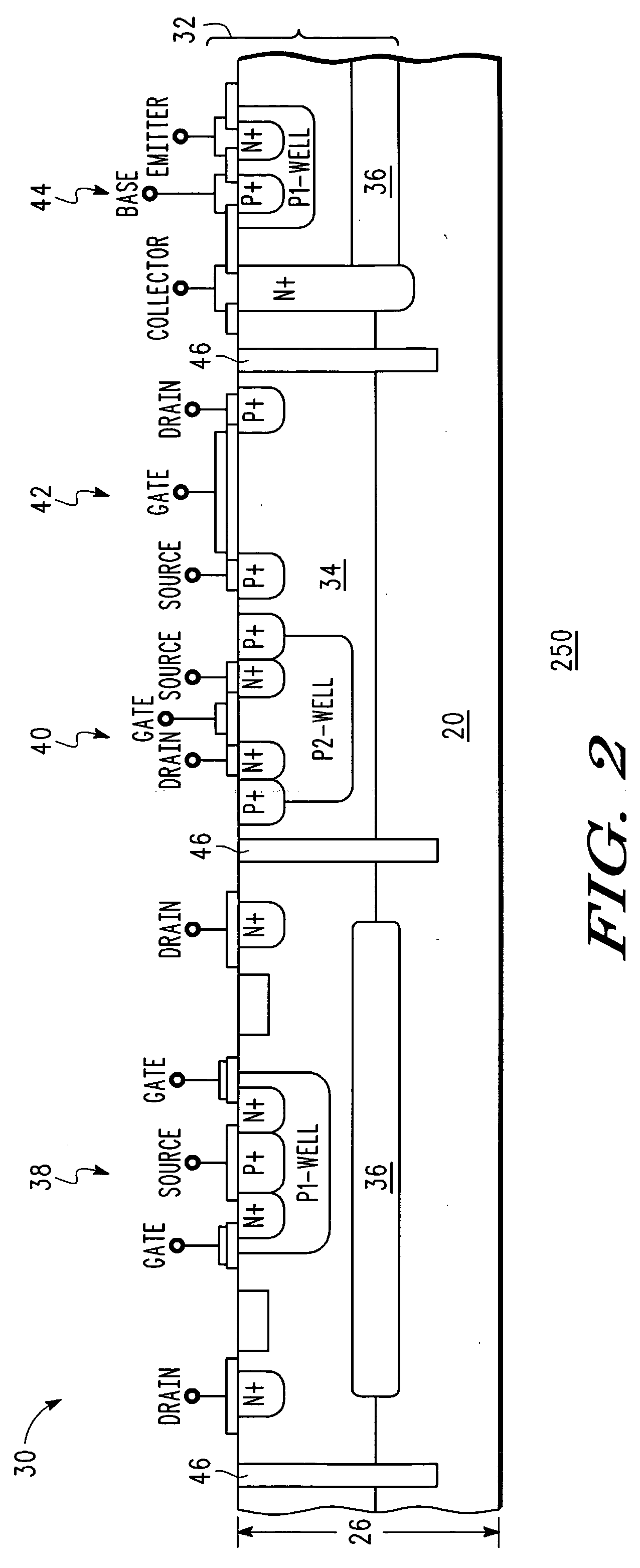
[0017]FIG. 2 illustrates one of the dies 30, or other portion of the substrate 20, along with an
integrated circuit 32 formed thereon. In one embodiment of the present invention, the
integrated circuit 32 is a “smart” power integrated circuit, as is commonly understood. As shown, the integrated circuit 32 (and / or the substrate 20) includes an N-type doped epitaxial layer 34, with N+ buried
layers 36 formed therein, and a power
metal-
oxide semiconductor field-effect
transistor (
MOSFET) 38, complementary
metal-
oxide semiconductor (
CMOS) devices (N-
MOSFET 40 and P-
MOSFET 42), and a bipolar device 44. The integrated circuits 32 may also include other various active and passive components, such as diodes, resistors, capacitors, inductors, fuses, anti-fuses, and memory devices, as well as at least one
metal layer, with additional metal
layers being added, to increase the circuit density and to enhance
circuit performance. As shown in FIG. 2, various N-type and P-type contact regions and wells are formed using known semiconductor
processing methods, such as implantation and
diffusion. In the depicted embodiment, the substrate 20 also includes isolation components 46, such as
shallow trench isolation (STI) regions, which may be formed using an oxidation and / or a trenching process.
[0030]The amorphous fixed ferromagnetic layer 108 is formed on the metallic
coupling layer 106, which overlies the pinned ferromagnetic layer 104. As used herein, the term “amorphous” shall mean a material or materials in which there is no long-range crystalline order such as that which would give rise to a readily discernable peak using normal x-
ray diffraction measurements or a discernable pattern image using
electron diffraction measurements. In one embodiment of the invention, amorphous fixed ferromagnetic layer 108 may be formed of an
alloy of
cobalt (Co), iron (Fe), and
boron (B). For example, the amorphous fixed layer 108 may be formed of an
alloy comprising 71.2% at.
cobalt, 8.8% at. iron, and 20% at.
boron. This composition is a CoFe
alloy with
boron added and may be represented as (Co89Fe11)80B20. However, it will be appreciated that any other suitable
alloy composition, such as CoFeX (where X may be one or more of
tantalum,
hafnium, boron, carbon, and the like), or alloys comprising
cobalt and / or iron, may be used to form amorphous fixed layer 30. The metallic
coupling layer 106 may be formed of any suitable material that serves to antiferromagnetically couple the crystalline pinned layer 104 and the amorphous fixed layer 108, such as
ruthenium,
rhenium,
osmium,
rhodium, or alloys thereof, but is preferably formed of
ruthenium. The metallic
coupling layer 106, the crystalline pinned layer 104, and the amorphous fixed layer 108 create a synthetic antiferromagnet (SAF) structure 114. The
antiferromagnetic coupling of the SAF structure 114 provided through the metallic coupling layer 106 improves the stability of the MTJ cell 88 in applied magnetic fields. Additionally, by varying the thickness of the ferromagnetic
layers 104 and 108, magnetostatic coupling to the free layer 110 can be offset and the
hysteresis loop can be centered.
[0031]The lack of substantial crystalline grain boundaries within the amorphous fixed layer 108 facilitates the growth of the
tunnel barrier layer 94 with a reduced
surface roughness compared to the
tunnel barrier layer 94 being grown over a crystalline or polycrystalline fixed layer. The smoother surfaces of the
tunnel barrier layer 94 improve the
magnetoresistance of the MTJ cell 88. In addition, the crystalline pinned layer 104 provides sufficient
antiferromagnetic coupling strength so that the SAF structure 114 is stable in an external
magnetic field. Accordingly, the amorphous fixed layer 108 and the crystalline pinned layer 104 serve to improve performance, reliability, and manufacturability of the MJT cell 88.
[0038]One
advantage of method and
system described above is that, because of the strongly
negative voltage coefficient of the MTJ memory cells, the MTJ cells provide superior sensitivity as voltage sensors. Another
advantage is that, because of the
high resistance of the MTJ cells, the amount of current required is minimized and power dissipation is reduced, thus increasing the efficiency of the microelectronic assembly. A further
advantage is that because the MTJ cells can be arranged in series, the
voltage sensing range of the assembly can be adjusted. The MTJ voltage sensors also demonstrate excellent voltage isolation capability, as they are formed during backend
processing, further improving the operation of the assembly. Additionally, because of the small size the MTJ cells, as well as the formation thereof during back end
processing, the space occupied by the
voltage sensing components, particularly on the semiconductor substrate, is minimized. Thus, the overall size of the assembly is reduced and performance is even further improved.

