Method for Rapid Liquid Phase Deposition of Crystalline Si Thin Films on Large Glass Substrates for Solar Cell Applications

a technology of crystalline si thin films and solar cells, applied in the direction of sustainable manufacturing/processing, final product manufacturing, coatings, etc., can solve the problems of low 14.78 tons of silicon needed, and 5-8% of the energy conversion efficiency of such cells, so as to increase the area throughput, the effect of equal energy conversion efficiency

Inactive Publication Date: 2008-10-02
SIERRA SOLAR POWER
View PDF6 Cites 15 Cited by
  • Summary
  • Abstract
  • Description
  • Claims
  • Application Information

AI Technical Summary

Benefits of technology

[0014]The presently preferred embodiment of the invention comprises a method for liquid phase deposition of crystalline Si thin films onto glasses, and the fabrication of high efficiency solar cells using crystalline silicon thin film technology. This deposition method enables rapid deposition of crystalline Si thin films on very large glass substrates with a deposition rate of up to 50 micron per minute. A solar cell that is fabricated on this crystalline Si thin film, as disclosed herein, that equal energy conversion efficiency to that of a cell that is made of a crystal Si wafer, but uses only 10% of the amount of silicon used by a wafer-based solar cell, considering the losses prior to reaching the final usable wafer thickness of ˜200 μm. Therefore, the solar cell based on this invention has the performance of a crystal silicon solar cell, but at a cost per unit area similar to that of a solar cell fabricated using an amorphous silicon thin film. Because of the maturity of silicon technology in semiconductor industry, this approach not only enables high volume, automatic production of solar cells on a very large, low-cost substrate, but also increases the area throughput up to 10000 cm2 / min from 942 cm2 / min in case of CZ crystal growth. With this approach, the manufacturing cost becomes much less sensitive to silicon price fluctuations, and the solar module cost is expected to be reduced to around $1 / Wp due to silicon material saving and factory output improvement. This is expected to provide a solar module that propels solar electricity penetration in the energy market.
[0016]In this embodiment of the invention, a 25-200 μm, but preferably 50-100 μm silicon film is deposited on a glass substrate. The silicon is first melted in a container, then dispensed through nozzles onto a moving heated substrate. The substrate is maintained at an elevated temperature for a specified time to reduce defects within the film. Dispensing of silicon onto the substrate is accomplished by controlling the capillary force, the pressure difference inside and outside of the container in which the silicon is melted, and the wetting property of the nozzle and the substrate. In one embodiment, the substrate is moved linearly at a rate of 1 cm / s or higher. The deposition thickness is controlled by factors that include the rate at which silicon is dispensed, the substrate wettability, the substrate moving rate, and substrate temperature. The glass substrates are chosen for its low cost, similar expansion coefficient to silicon, and high light transmission.

Problems solved by technology

For each MW electricity output, 14.78 tons of silicon is needed because of losses that result from the manufacturing process.
The recent supply shortage and price hiking of silicon feedstock also creates a hurdle to the growth of the solar cell industry.
However, the technology maturity, the toxicity of the materials used to manufacture such cells, and the limited availability of materials used to manufacture such cells, such as indium, tellurium, and selenium, are casting a shadow on the future of these types of solar cell.
However, the energy conversion efficiency of such cells is low (˜5-8%) due to low carrier mobility in amorphous silicon and the thin film thickness.
The film has to be thin for photon generated carriers to reach the collecting electrodes due to low carrier lifetime and mobility.
The thin a-silicon film cannot absorb the solar energy effectively due to low absorption coefficient and band gap mismatch with solar spectrum.
The energy conversion efficiency of such cell also degrades as the level of hydrogen within the film decreases.
However, it is difficult to handle this material in the form of stand-alone wafers.
On the other hand, there is no effective method for producing 50-100 um thin film solar cells at a production-worthy rate.
However, the films formed in this method are rather thick, on the order of 0.5 mm.
This increases cost and also may result in reliability problems due to thermal mismatches.

Method used


Image

  • Method for Rapid Liquid Phase Deposition of Crystalline Si Thin Films on Large Glass Substrates for Solar Cell Applications
  • Method for Rapid Liquid Phase Deposition of Crystalline Si Thin Films on Large Glass Substrates for Solar Cell Applications
  • Method for Rapid Liquid Phase Deposition of Crystalline Si Thin Films on Large Glass Substrates for Solar Cell Applications

Examples


Embodiment Construction

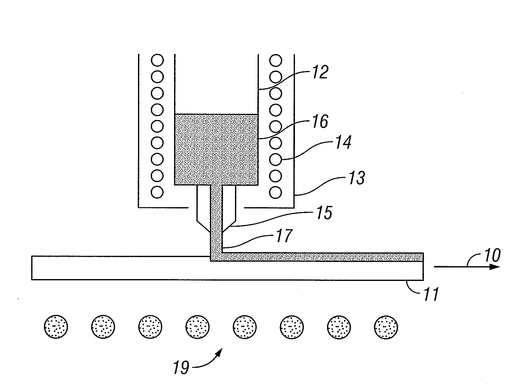
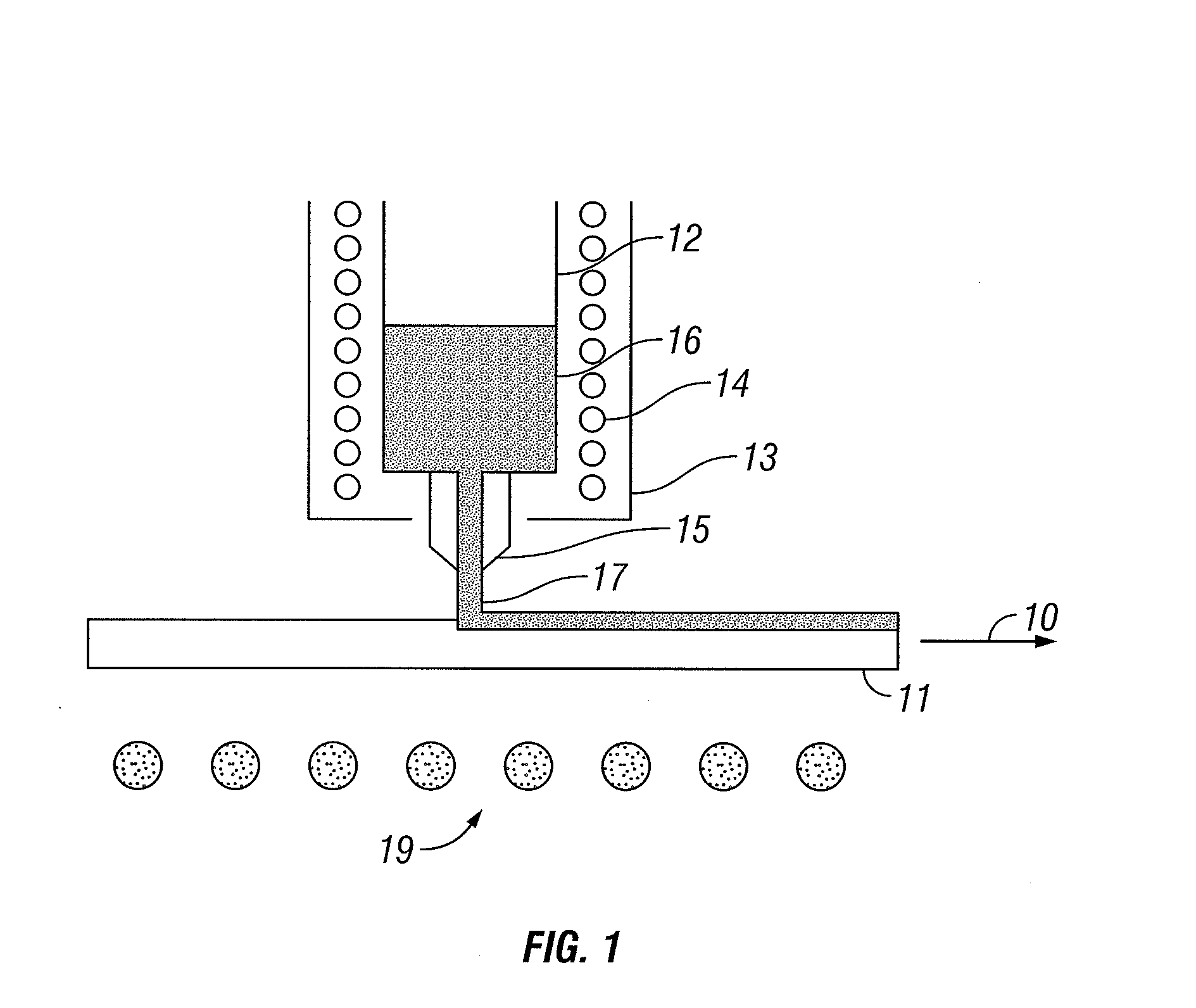
[0025]The presently preferred embodiment of the invention comprises a method for liquid phase deposition of crystalline Si thin films onto glass. A solar cell that is fabricated using the invention disclosed herein has the performance of a crystal silicon solar cell, but at per unit area cost that is similar to that of a solar cell that is fabricated using an amorphous silicon thin film. In the fabrication of a conventional crystal Si solar cell, although the wafer thickness used is slightly below 200 μm, there are significant losses from raw material to the wafers, such as growth, cutting, and polishing. In the invention, the crystal thin film uses only 10% of the amount of silicon used by a wafer-based solar cell per unit area. The cell manufacturing process follows existing Si processing techniques. Because of the maturity of silicon technology in semiconductor industry, this approach not only enables high volume, automated production of solar cells on a very large, low-cost subs...


PUM

PropertyMeasurementUnit
thicknessaaaaaaaaaa
thicknessaaaaaaaaaa
grain sizeaaaaaaaaaa

Abstract

A method for liquid phase deposition of crystalline silicon thin films, and a high efficiency solar cell that is fabricated using crystalline silicon thin film technology, has the performance of a crystal silicon solar cell, but at the cost level per unit area of a solar cell fabricated using an amorphous silicon thin film. The crystal thin film uses only 10% or less of the amount of silicon used in a wafer-based solar cell. Because of the maturity of silicon technology in semiconductor industry, this approach not only enables high volume, automated production of solar cells on a very large, low-cost substrate, but also increases the area throughput up to 10000 cm2 / min from 942 cm2 / min in case of CZ crystal growth.

Description

BACKGROUND OF THE INVENTION[0001]1. Technical Field[0002]The invention relates to liquid phase deposition of crystalline Si thin films and solar cells. More particularly, the invention relates to a high efficiency solar cell that is fabricated using crystalline silicon thin film technology.[0003]2. Description of the Prior Art[0004]Rising fuel costs and increasing worldwide energy demands have created a need for alternatives to conventional, e.g. hydrocarbon-based, sources of energy. Solar generated electricity is becoming a practical solution that addresses the increasing energy demand and may eventually replace the conventional hydrocarbon fueled power plant. Currently, solar electricity only accounts for 1.5% of the 5000 GW electricity market. The total available market for solar cells reached $4B in 2005 and is increasing rapidly, with a CAGR of 25-30% for the next ten years.[0005]A simple solar cell consists of two layers of semiconductor material, typically silicon, sandwiched...

Claims


Application Information

Patent Timeline
Patent Type & Authority Applications(United States)
IPC IPC(8): H01L31/00B05C11/00B05D5/12C23C14/54
CPCC23C6/00H01L31/03921H01L31/1824Y02E10/545Y02P70/50
Inventor FU, JIANMINGXU, ZHENG
Owner SIERRA SOLAR POWER
Why Eureka
Try Eureka