

Semiconductor device and method for manufacturing the same
a semiconductor and semiconductor technology, applied in the direction of identification means, instruments, optics, etc., can solve the problems of glass substrate warpage, adverse effects of transistor characteristics, strain stress applied to single-crystal silicon layer, etc., to reduce the effect of surface contamination, preventing contamination of semiconductor substrates, and reducing localized level density
- Summary
- Abstract
- Description
- Claims
- Application Information
AI Technical Summary
Benefits of technology
Problems solved by technology
Method used
Image

Examples
embodiment mode 1
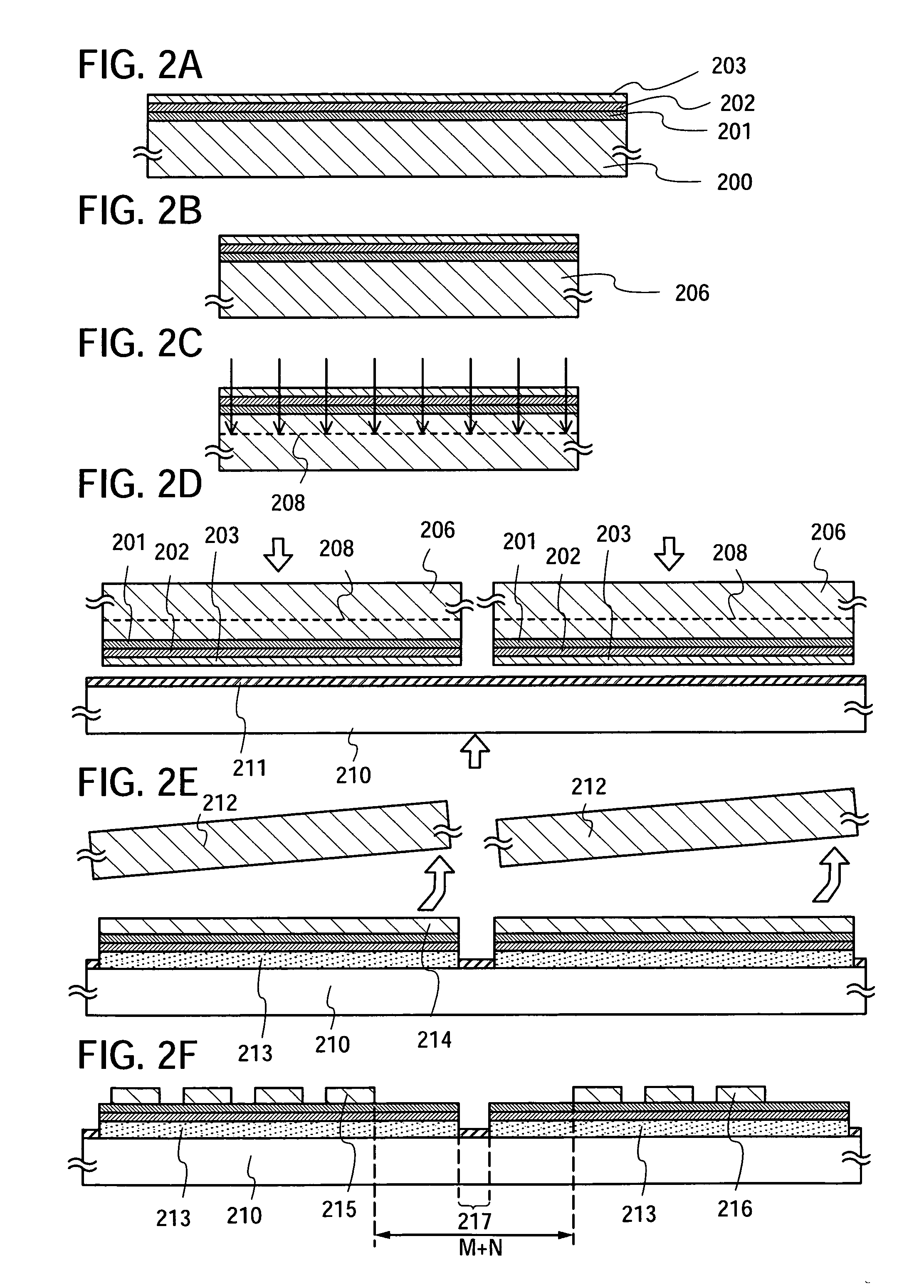
[0063]First, a top view of a semiconductor substrate 200 which has a thin circular shape is shown in FIG. 3A. As is shown in FIG. 3A, the semiconductor substrate 200 has a flat as a part of its rim to indicate crystallographic orientation. Here, a 5-inch silicon wafer (125 mm in diameter) is used as an example. Note that an 8-inch silicon wafer (200 mm in diameter) or a 12-inch silicon wafer (300 mm in diameter) can be used if needed.
[0064]A silicon oxynitride layer 201 is formed over the semiconductor substrate 200. A thickness of the silicon oxynitride layer 201 may be set as appropriate by a practitioner and may be 10 to 500 nm (preferably 10 to 150 nm). The silicon oxynitride layer 201 later serves as a part of an insulating layer in an SOI substrate. Note that the silicon oxynitride layer 201 can be formed by a method such as a CVD method like a plasma CVD method or a low pressure CVD method, or a sputtering method. For example, the silicon oxynitride layer 201 can be formed ov...
embodiment mode 2
[0151]This embodiment mode describes a method for manufacturing an SOI substrate which includes steps different from the steps in FIGS. 2A to 2F below.
[0152]In FIG. 6A, a p-type or an n-type single crystal silicon substrate (silicon wafer) is typically used as a semiconductor substrate 400.
[0153]Then, the semiconductor substrate 400 is ground or cut so as to be a rectangle sheet 406.
[0154]Then, degreasing washing is performed on the sheet 406 and an oxide film on the surface is removed and thermal oxidation is performed. As thermal oxidation, normal dry oxidation may be performed; however, oxidation in an oxidation atmosphere in which a halogen is added is preferably performed. For example, thermal treatment is performed at a temperature of equal to or higher than 700° C. in an atmosphere containing HCl at 0.5 to 10 volume % (preferably 3 volume %) with respect to oxygen. Preferably, thermal oxidation may be performed at a temperature of 950 to 1100° C. The processing time may be 0....
embodiment mode 3
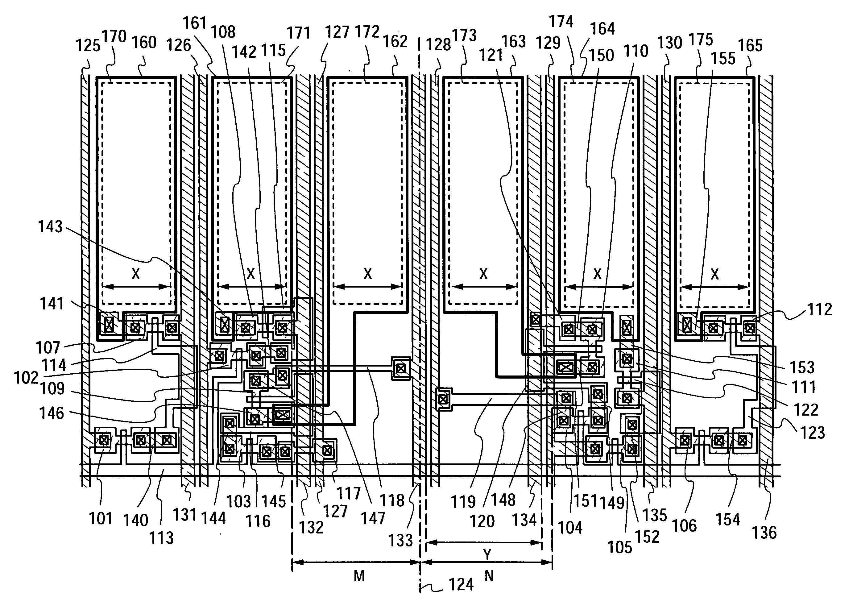
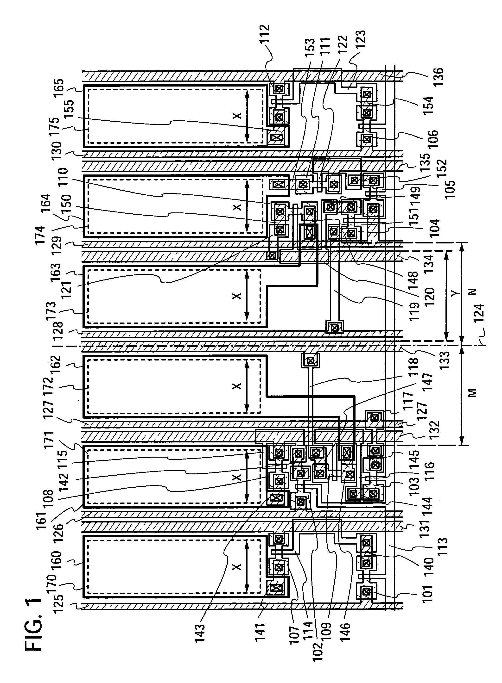
[0177]This embodiment mode describes an example in which a semiconductor device is manufactured using a plurality of single-crystal semiconductor layers which are disposed over a support substrate, which are manufactured according to Embodiment Mode 1 or Embodiment mode 2.
[0178]A semiconductor device having a light emitting element can be formed according to the present invention, and the light emitting element emits light by any one of bottom emission, top emission, or dual emission. This embodiment mode describes an example of a method for manufacturing a semiconductor device with high yield, in which a semiconductor device having a display function (also referred to as a display device or a light emitting device) is manufactured as a bottom-emission, dual-emission, or top-emission semiconductor device with high performance and high reliability, with reference to FIGS. 7A, 7B, and 8.
[0179]First, island-shaped single-crystal semiconductor layers are formed over a support substrate ...
PUM
| Property | Measurement | Unit |
|---|---|---|
| temperature | aaaaa | aaaaa |
| size | aaaaa | aaaaa |
| size | aaaaa | aaaaa |
Abstract
Description
Claims
Application Information