Nanoparticle Synthesis and Associated Methods

a nanoparticle and nanoparticle technology, applied in the direction of organic chemistry, polycrystalline material growth, crystal growth process, etc., can solve the problems of poor nucleation process, large quantity, and limited industrialization of nanoscale materials, so as to promote more efficient annealing, increase the quantum efficiency of out-of-batch, and increase the quantity

Active Publication Date: 2008-12-04
FLORIDA STATE UNIV RES FOUND INC
View PDF21 Cites 22 Cited by
  • Summary
  • Abstract
  • Description
  • Claims
  • Application Information

AI Technical Summary

Benefits of technology

[0015]It is believed that superheating, which results in reaction pressurization and changes in the dielectric constant of the reactants, promotes more efficient annealing at the surface of the nanoparticle, giving rise to larger quantities (>1 kg), higher out-of-batch quantum efficiencies (QE>70%), greater crystallinity, more rapid growth (<1 m), and ease of isolation of nanocrystals from alkane solvents (hexane, heptane, octane, nonane, decane, dodecane, etc.). The lower-boiling-point solvents allow larger nanocrystals to be generated. In addition, shape control (rods, spheres, tetrapods) has been demonstrated depending on the nature of the starting materials or additives. The invention is believed to mimic the bulk semiconductor growth conditions where metallic salts are heated to temperatures in excess of 1000° C.
[0016]Microwave heating of group-12 and -13 organometallic precursors and group-15 and -16 reactants has demonstrated that dielectric heating is a viable method for the preparation of high-quality photoluminescent semiconducting nanoparticles. Additives, for example, tri-octyl phosphine oxide (TOPO) or ionic liquids, can have a dramatic effect on the observed growth behavior in the microwave. Increasing microwave power increases the reaction rate and material quality owing to overcoming kinetic barriers. This is believed to represent a significant step towards the commercial availability of III-V phosphors.
[0017]The present invention indicates that multiple sizes of CdSe and the more delicate III-V colloidal semiconductor nanoparticles can be rapidly synthesized in a closed system by microwave-assisted synthesis in less than 20 min with no sacrifice to the structure or optical quality. This method can be tailored to existing synthetic routes utilizing high-boiling solvents. It is also sho

Problems solved by technology

As nanoscale devices become more of a commercial reality, the industrialization of nanoscale materials has been limited by the need for new material compositions and the development of high-throughput automation for materials preparation.
The formation of nanocrystals is notorious for its difficulty and required long reaction times, on the order of hours.
Further, for large-scale reactions inhomogeneities in the growth process can be magnified by thermal gradients in the reaction, which produce poor nucleation processes and therefore broadened size di

Method used


Image

  • Nanoparticle Synthesis and Associated Methods
  • Nanoparticle Synthesis and Associated Methods
  • Nanoparticle Synthesis and Associated Methods

Examples


Embodiment Construction

[0038]A description of the preferred embodiments of the present invention will now be presented with reference to FIGS. 1-15B.

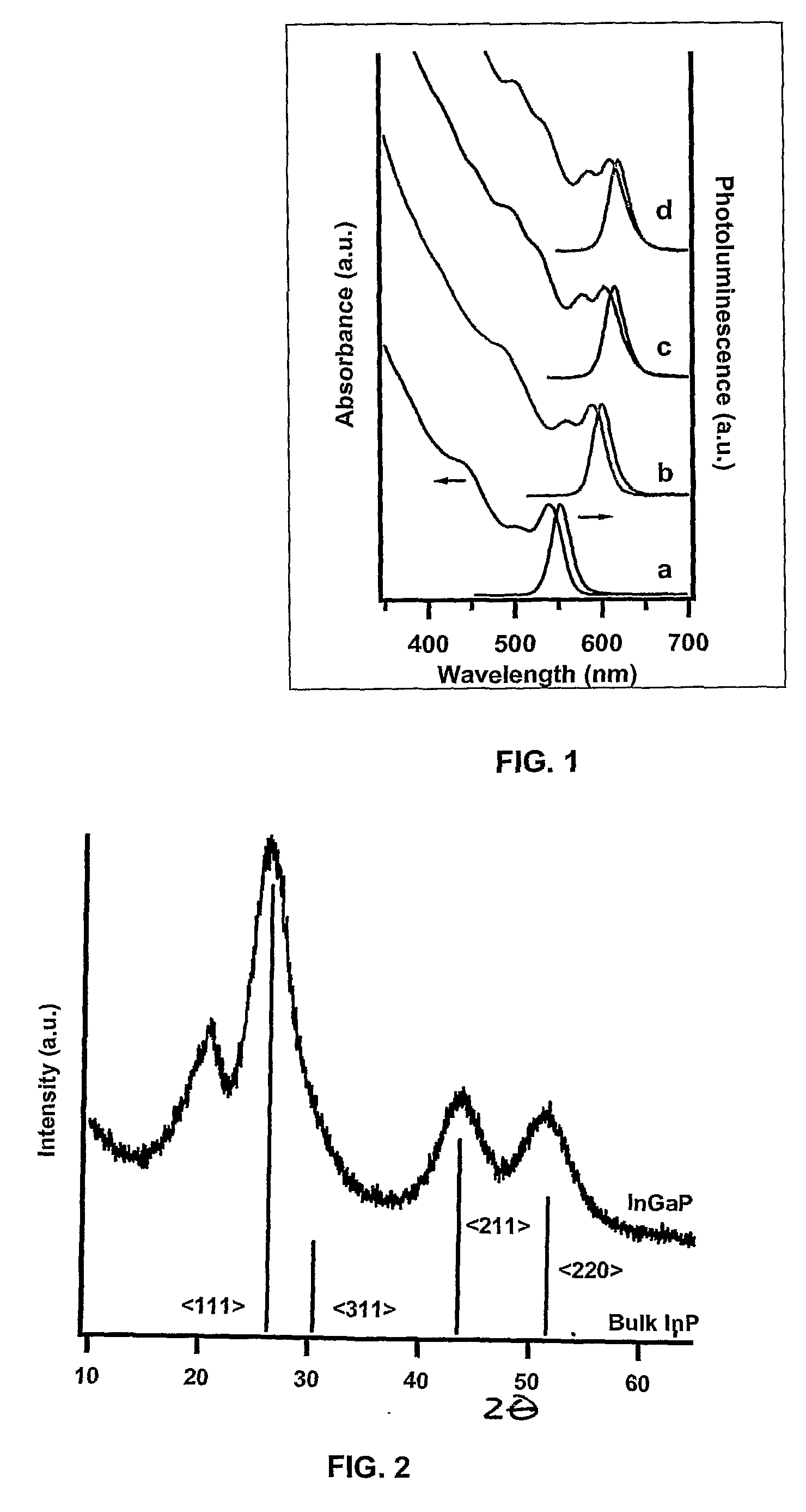
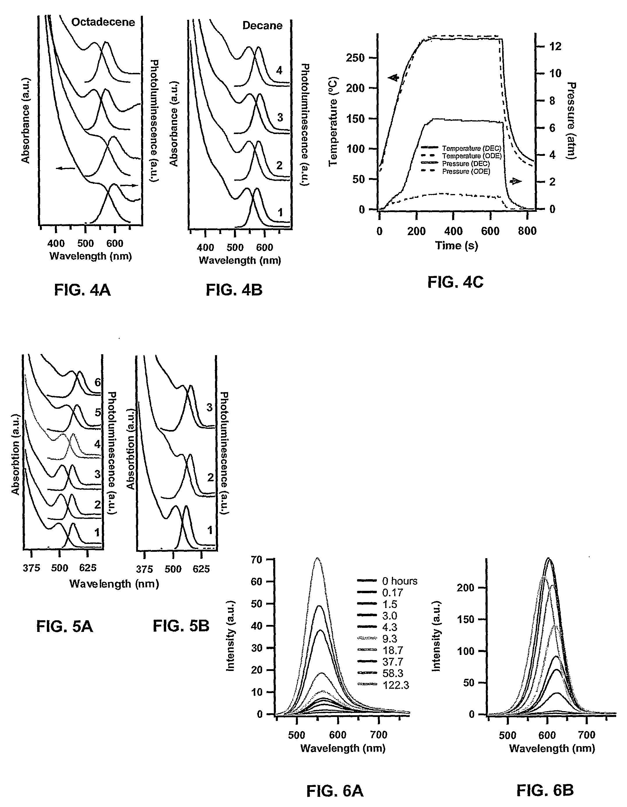
[0039]The method of the present invention demonstrates that microwave heating methods can address the problem of heating inhomogeneity in forming nanoparticle materials, while providing a scalable platform for industrial applications. Microwave heating has been demonstrated to enhance reaction rates, selectivity, and product yields in organic chemistry. By judicious choice of the solvents, passivating ligands, and reactants, the nanomaterial precursors can be selectively heated over the solvent or passivating ligand. Selective heating in the microwave cavity is advantageous in organic synthesis, and in general these microwave synthetic methodologies are quite adaptable to reactions that have high energies of activation and slow reaction rates. This effect confers advantages for colloidal nanostructured materials synthesis.

[0040]The present invention is direct...


PUM


Abstract

A method is provided for producing crystalline nanoparticle semiconductor material. The method includes the steps of mixing a precursor in a solvent to form a reaction mixture and subjecting the reaction mixture to microwave dielectric heating at sufficient power to achieve a superheating temperature of the reaction mixture. A growth-phase reaction is permitted to proceed, wherein nanoparticles are formed in the heated reaction mixture. The reaction is then quenched to substantially terminate nanoparticle formation.

Description

BACKGROUND OF THE INVENTION[0001]1. Field of the Invention[0002]The present invention relates to systems and methods for synthesizing nanoparticles, and, more particularly, to such systems and methods utilizing microwave energy.[0003]2. Description of Related Art[0004]New applications and technology for nanoscale semiconducting and metallic nanoparticles have grown owing to advancements in the chemical synthetic methodologies for their preparation. These materials are being utilized in applications including as bio-markers, in solar cells, and in lighting technologies, for example. As nanoscale devices become more of a commercial reality, the industrialization of nanoscale materials has been limited by the need for new material compositions and the development of high-throughput automation for materials preparation.[0005]The formation of nanocrystals is notorious for its difficulty and required long reaction times, on the order of hours. Further, for large-scale reactions inhomogene...

Claims


Application Information

Patent Timeline
IPC IPC(8): B01J19/12
CPCB82Y30/00B82Y40/00C01B31/0226C01B31/06C01G1/02C01G15/00C01P2002/72C01P2004/64C30B7/00C30B29/60H01L21/02521H01L21/02543H01L21/02554H01L21/0256H01L21/02601H01L21/02606C01B32/16C01B32/25C01B32/26
Inventor STROUSE, GEOFFREY F.GERBEC, JEFFREY A.
Owner FLORIDA STATE UNIV RES FOUND INC
Why Eureka
Try Eureka