Nitride semiconductor stacked structure and semiconductor optical device, and methods for manufacturing the same

a technology of stacked structure and semiconductor, which is applied in the direction of lasers, nanoinformatics, semiconductor lasers, etc., can solve the problems of (n) desorption, complex manufacturing process, and crystal degradation, and achieve the effect of low resistance, low resistance, and low resistan

Active Publication Date: 2009-01-08
MITSUBISHI ELECTRIC CORP
View PDF5 Cites 12 Cited by
  • Summary
  • Abstract
  • Description
  • Claims
  • Application Information

AI Technical Summary

Benefits of technology

[0018]The present invention has been made so as to solve the above problem and a first object is to provide a nitride semiconductor stacked structure comprising a p-type nitride semiconductor layer of low resistance which is formed by use of a Group III material of an organometallic compound and Group V materials including a hydrazine derivative. A second object is to provide a semiconductor light-emitting device comprising a p-type nitride semiconductor layer of lower resistance formed by using a Group III material of an organometallic compound and Group V materials including a hydrazine derivative. A third object is to provide a method for manufacturing, by a simple process, a nitride semiconductor stacked structure comprising a p-type nitride semiconductor layer of low resistance by using a Group III material of an organometallic compound and Group V materials including a hydrazine derivative. A fourth object is to provide a method for manufacturing, by a simple process, a semiconductor light-emitting device comprising a p-type nitride semiconductor layer of low resistance by using a Group III material of an organometallic compound and Group V materials including a hydrazine derivative.

Problems solved by technology

However, when the thermal treatment is carried out, there may be some possibility that nitrogen (N) desorbed from the surface of the p-type semiconductor layer, thereby degrading the crystal.
This needs annealing so as to increase the activity rate of the p-type dopant when NH3 is used, and thus, not only the manufacturing process becomes complicated, but also there is the possibility that nitrogen (N) desorbs from the surface of the p-type semiconductor to degrade the crystal.
On the other hand, when a material incapable of generating a H radical, e.g. dimethylhydrazine (UDMHy), is used as a Group V material in place of NH3 and a Group III material of an organometallic compound is used, carbon (C) is taken in the crystal, with the attendant problem that there is some possibility that the resulting p-type semiconductor layer exhibits a high resistance.

Method used


Image

  • Nitride semiconductor stacked structure and semiconductor optical device, and methods for manufacturing the same
  • Nitride semiconductor stacked structure and semiconductor optical device, and methods for manufacturing the same
  • Nitride semiconductor stacked structure and semiconductor optical device, and methods for manufacturing the same

Examples


first embodiment

[0036]FIG. 1 is a schematic view showing a section of a GaN stacked structure according to one embodiment of the present invention. It will be noted that like reference numerals indicate corresponding or like members throughout the drawings.

[0037]In FIG. 1, a GaN stacked structure 10 constitutes, for example, part of a stacked structure of blue-violet LD.

[0038]A GaN substrate 12 serving as a substrate makes use of a (0001) face as a main surface and a p—GaN layer 14 serving as a p-type nitride semiconductor layer is disposed on this main surface.

[0039]The manufacturing procedure of the GaN stacked structure 10 is illustrated.

[0040]In general, the crystal growth for forming a nitride semiconductor stacked structure is carried out by a metal organic chemical vapor deposition (MOCVD) method, molecular beam epitaxy (MBE), hydride vapor phase epitaxy (HVPE) or the like. The MOCVD method is, for example, used herein.

[0041]Trimethylgallium (TMGa), which is an organometallic compound, is us...

modification 1

[0071]In the manufacturing steps set out hereinabove, the case where nitrogen (N2) gas alone is used as a carrier gas for starting gases has been illustrated, there may be used, as a carrier gas, a mixed gas of nitrogen (N2) gas and hydrogen (H2) gas, or hydrogen (H2) gas alone.

[0072]More particularly, when a compositional ratio by volume of hydrogen gas is taken as x and a compositional ratio by volume of nitrogen gas is taken as 1-x, the manufacture is feasible using a mixed gas of hydrogen gas and nitrogen gas within a range of 1=x=0.

[0073]For instance, where hydrogen gas and nitrogen gas are mixed at 1:1 to provide a mixed gas, the nitrogen gas is fed at a feed flow rate of 10 liters / minute and the hydrogen gas is fed at a feed flow rate of 10 liters / minute to provide a mixed gas.

[0074]Other manufacturing conditions are the same as those manufacturing conditions using nitrogen gas alone as a carrier gas.

[0075]It has been found that when the p—GaN layer of Modification 1 made by ...

second embodiment

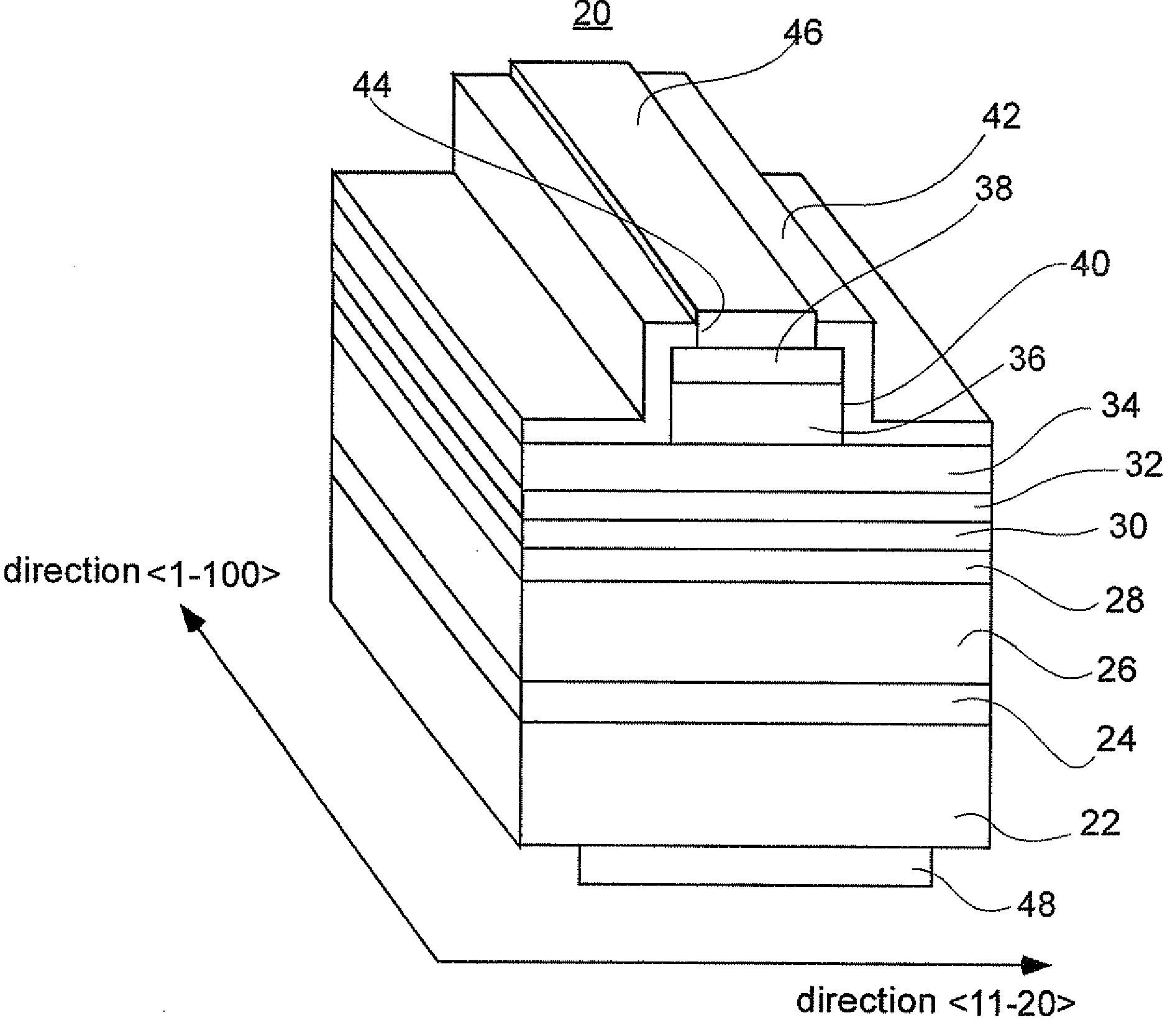
[0097]FIG. 6 is a perspective view of LD according to one embodiment of the present invention.

[0098]In FIG. 6, LD 20 is a blue-violet LD having a ridge-type waveguide and includes a n—GaN substrate 22 used as a substrate. There are successively stacked, on a (0001) face serving as a main surface of the n—GaN substrate 22, a 1 μm thick buffer layer 24 made of n—GaN, a 1.0 μm thick cladding layer 26 formed of n—Al0.07Ga0.93N on the buffer layer a 0.1 μm thick n-side optical guide layer 28 made of n—GaN on the n-cladding layer and an active layer 30.

[0099]The active layer 30 has a multiple quantum well structure provided with three pairs of 3.5 μm thick well layers made of In0.12Ga0.88N and 7.0 nm thick barrier layers made of GaN, which are alternately stacked.

[0100]There are successively formed, over the active layer 30, a 0.2 μm thick p-type electron barrier layer 32 formed of p—Al0.07Ga0.93N and a 0.1 μm thick p-side optical guide layer 34 formed of p—GaN. Next, a 0.4 μm thick p-cla...


PUM

PropertyMeasurementUnit
temperatureaaaaaaaaaa

Abstract

A nitride semiconductor stacked structure having good working efficiency includes a p-type nitride semiconductor layer of low resistance, which is formed from an organometallic compound, compounds including Group V elements, including ammonia and a hydrazine derivative, and a p-type impurity material on a substrate. The p-type nitride layer has a carbon concentration not higher than 1×1018 cm−3.

Description

BACKGROUND OF THE INVENTION[0001]1. Field of the Invention[0002]The present invention relates to a nitride semiconductor stacked structure and a semiconductor optical device, and methods for manufacturing the same. More particularly, the invention relates to a nitride semiconductor stacked structure and a semiconductor optical device, both formed by use of Group V materials including ammonia and a hydrazine derivative and a Group III material of an organometallic compound and also to methods for manufacturing the same.[0003]2. Description of the Related Art[0004]Recently, extensive studies and developments of semiconductor lasers capable of light emission ranging from a blue region to a ultraviolet region have been made for high densification of optical disks. For GaN compound semiconductors used as such a blue to violet region diode (laser diode being referred to hereinafter as LD), mentions is made, for example, of GaN, GaPN, GaNAs, InGaN, AlGaN, AlGaInN and the like. GaN semicond...

Claims


Application Information

Patent Timeline
Patent Type & Authority Applications(United States)
IPC IPC(8): H01L33/00B82Y10/00B82Y20/00B82Y40/00H01L21/205H01S5/343
CPCB82Y20/00H01L21/0254H01L21/02576H01L21/02579H01L21/0262H01L33/325H01S2304/04H01S5/2009H01S5/22H01S5/2201H01S5/3054H01S5/34333H01S5/0202
Inventor OHNO, AKIHITOTAKEMI, MASAYOSHITOMITA, NOBUYUKI
Owner MITSUBISHI ELECTRIC CORP
Why Eureka
Try Eureka