

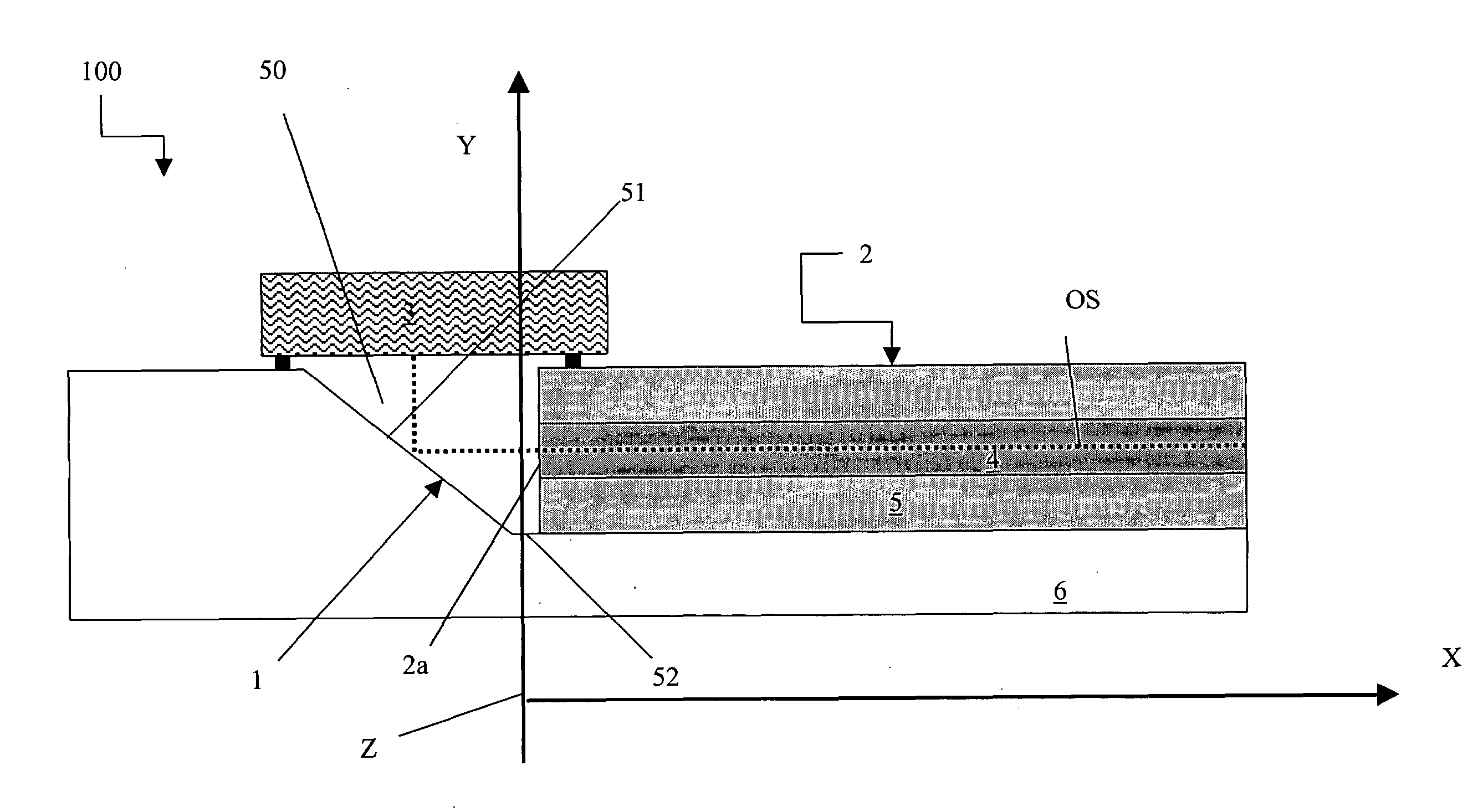
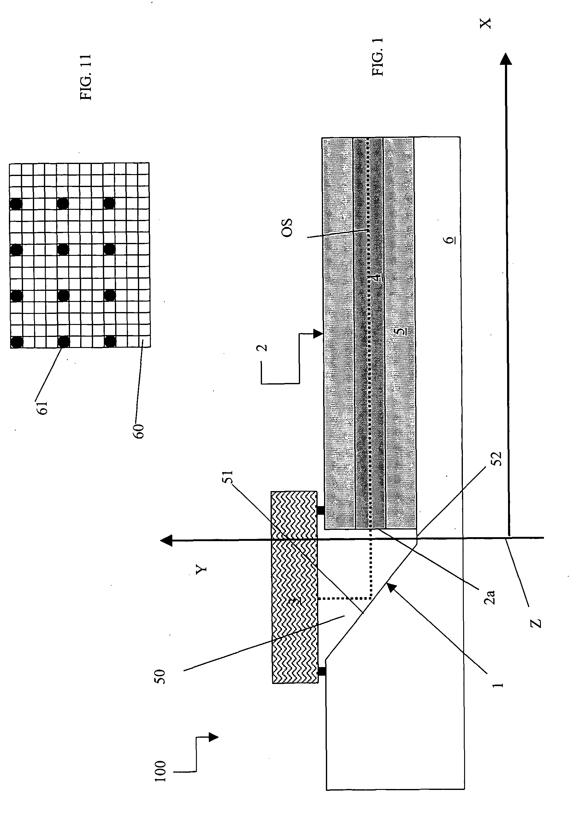
Method to Fabricate a Redirecting Mirror in Optical Waveguide Devices
a technology of optical waveguide and turning mirror, which is applied in the direction of photomechanical equipment, instruments, originals for photomechanical treatment, etc., can solve the problems of minimum usable pixel size, limited flexibility of etching method to fabricate turning mirror, and inconvenient use, so as to reduce the roughness of the resist sloped surface
- Summary
- Abstract
- Description
- Claims
- Application Information
AI Technical Summary
Benefits of technology
Problems solved by technology
Method used
Image

Examples
example 1
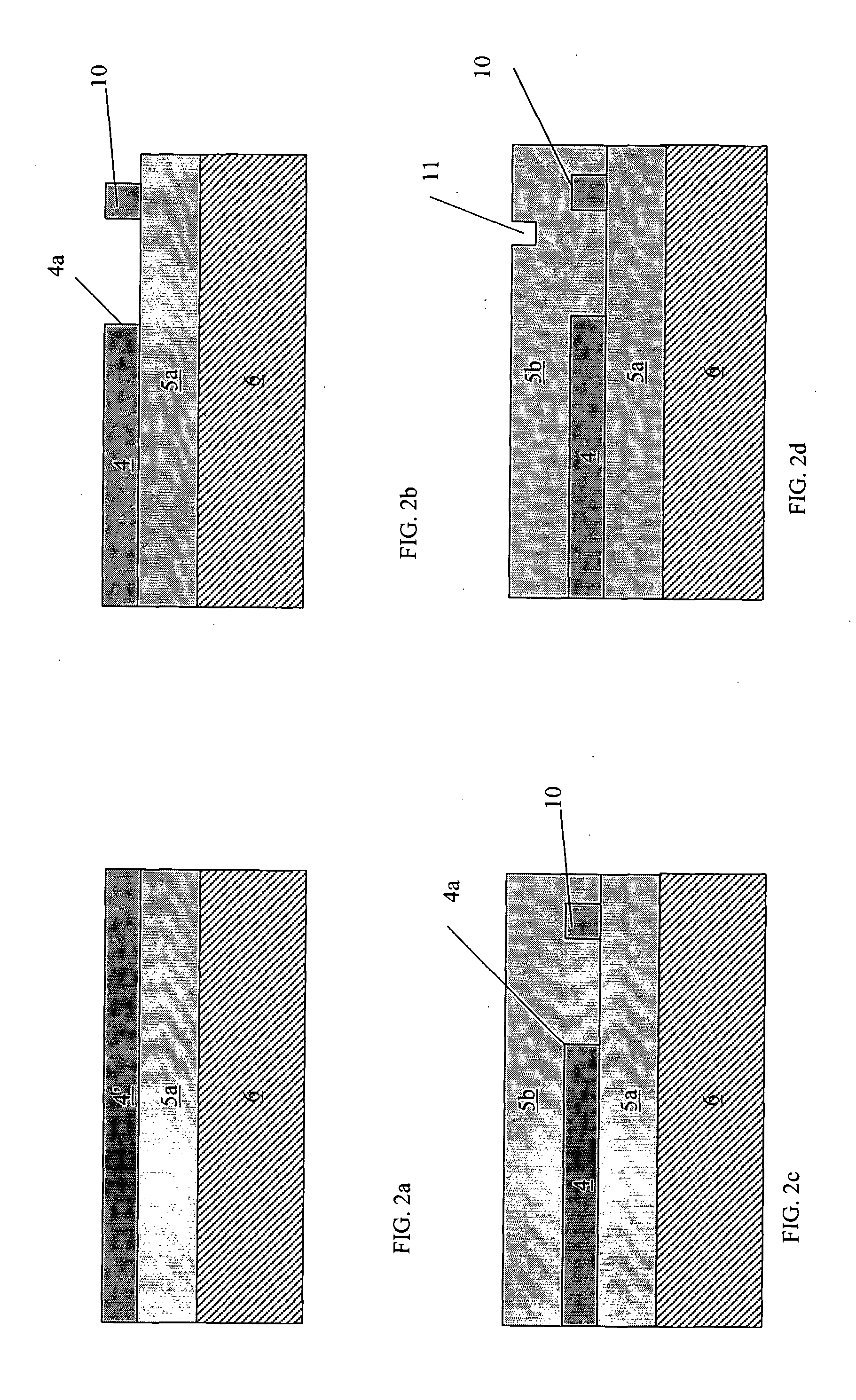
[0121]The turning mirror 1 of FIG. 7 is obtained according to the following example.
[0122]A 10 μm thick silicon dioxide (SiO2) layer (the lower cladding 5a) is firstly formed by thermal treatment on a silicon substrate, with a refractive index of 1.4585 at 633 nm, to act as the lower cladding. Alternatively, a poorly phosphorus-doped SiO2 layer (PTEOS) can be deposited by Chemical Vapour Deposition (CVD). Then a 2÷3 μm thick Ge-doped SiO2 layer 4′ is grown by CVD on top of the lower cladding, with a refractive index of 1.4949÷1.5241 at 633 nm (2.5%÷4.5% index contrast), to act as the waveguide core 4. The core layer 4′ is then patterned by means of optical lithography (using a suitable photomask and a UV sensitive photoresist) and Reactive Ion Etching (RIE). During this step, alignment marks 10 are formed. Afterwards, a 8÷10 μm thick boron and phosphorus doped silicon dioxide (BPSG or BPTEOS) layer is grown by CVD on top of and around the core layer, with a refractive index of 1.458...
PUM
| Property | Measurement | Unit |
|---|---|---|
| Length | aaaaa | aaaaa |
| Thickness | aaaaa | aaaaa |
| Thickness | aaaaa | aaaaa |
Abstract
Description
Claims
Application Information