Indium phosphide substrate, indium phosphide single crystal and process for producing them

a technology of indium phosphide and substrate, which is applied in the direction of non-metal conductors, conductors, polycrystalline material growth, etc., can solve the problems of high frequency of twin generation, difficult to obtain monocrystals, and difficult to achieve monocrystals, etc., to achieve adequate strength, prevent polycrystallization, and large deformation

Inactive Publication Date: 2009-03-19
SUMITOMO ELECTRIC IND LTD
View PDF8 Cites 15 Cited by
  • Summary
  • Abstract
  • Description
  • Claims
  • Application Information

AI Technical Summary

Benefits of technology

[0033]When using a seed crystal with larger diameter having a cross-sectional area of 15% or greater, and preferably 50% or greater of the cross-sectional area of the crystal body, using a crucible of material which easily deforms such as quartz results in a larger deformation as compared to when using a seed crystal with smaller diameter. Therefore, a pBN crucible which has adequate strength at growth temperatures is preferred. In addition, with a pBN crucible, if the inner surface of the crucible is not coated with boron oxide (B2O3), the crystal or the melt will come into contact with the crucible and polycrystallization occurs. When using a seed crystal with larger diameter having a cross-sectional area of 15% or greater, and preferably 50% or greater of the cross-sectional area of the crystal body, the surface area of the seed crystal is large as compared to the seed crystal with smaller diameter. As a result, there is a higher possibility of the crystal or the melt coming in contact with the crucible. Prior to housing the seed crystal, indium phosphide raw material, dopant, and boron oxide in the growth container, the inner surface of the growth container, at least the part which will come into contact with the melt, is coated with a boron oxide film, thereby preventing contact of the crystal or the melt with the crucible and preventing polycrystallization.
[0034]In this manner, an InP monocrystal with a diameter of 75 mm or greater and also 100 mm or greater containing a dopant of iron (Fe), sulfur (S), tin (Sn), or zinc (Zn) is obtained. In addition, this crystal is processed to obtain an InP substrate for use in optoelectronic devices such as semiconductor laser for optical communication, photodetector, and the like and electronic devices such as transistor and the like. This results in compound semiconductor devices with uniform and stable performance on the wafer and excellent life span.

Problems solved by technology

In the growth of InP crystals, twin generation is the most serious problem.
In particular, with the vertical boat method in which crystals are grown in containers such as VGF method and vertical Bridgman method (VB method), when crystals are grown under a low temperature gradient, there is a high frequency of twin generation, and it is extremely difficult to obtain a monocrystal.
As a result, there results a large gradient for the dopant concentration on the wafer.
As a result, when this is used for optoelectronic devices such as semiconductor lasers for optical communication, photodetectors, and the like, and for electronic devices such as transistors and the like, the performance of the device is not constant on the wafer.
However, if the growth speed is too fast, constitutional supercooling occurs, which results in polycrystallization.
However, with this method in which dopant is diffused from the atmosphere, this may result in dopant concentrations higher in areas closer to the wafer surface.
As a result, when using for optoelectronic devices such as semiconductor lasers for optical communication, photodetectors, and the like, and for electronic devices such as transistors and the like, the device performance may not be stable.
With an InP substrate used in the optoelectronics field such as semiconductor lasers for optical communication, photodetectors, and the like, dislocation reduces the device performance and life span.
Substrates with such a high dislocation density are problematic for practical use.

Method used


Image

  • Indium phosphide substrate, indium phosphide single crystal and process for producing them
  • Indium phosphide substrate, indium phosphide single crystal and process for producing them
  • Indium phosphide substrate, indium phosphide single crystal and process for producing them

Examples


embodiment 1

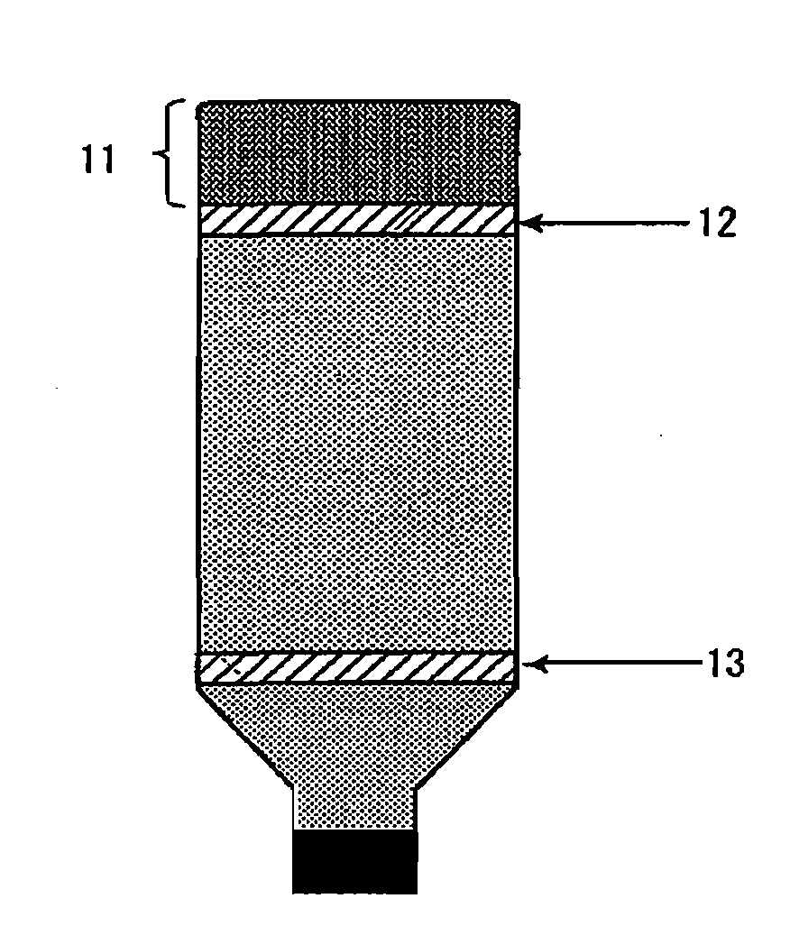
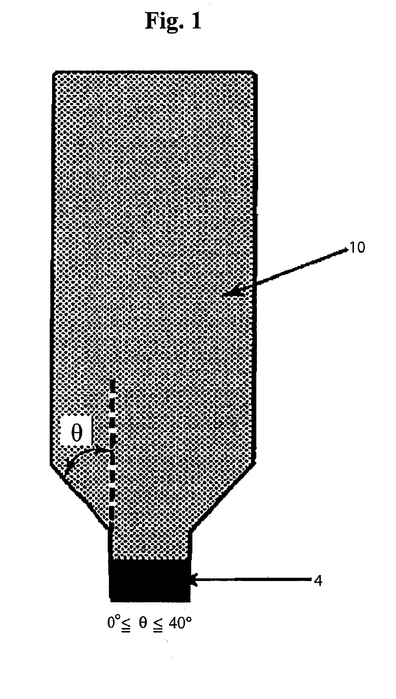
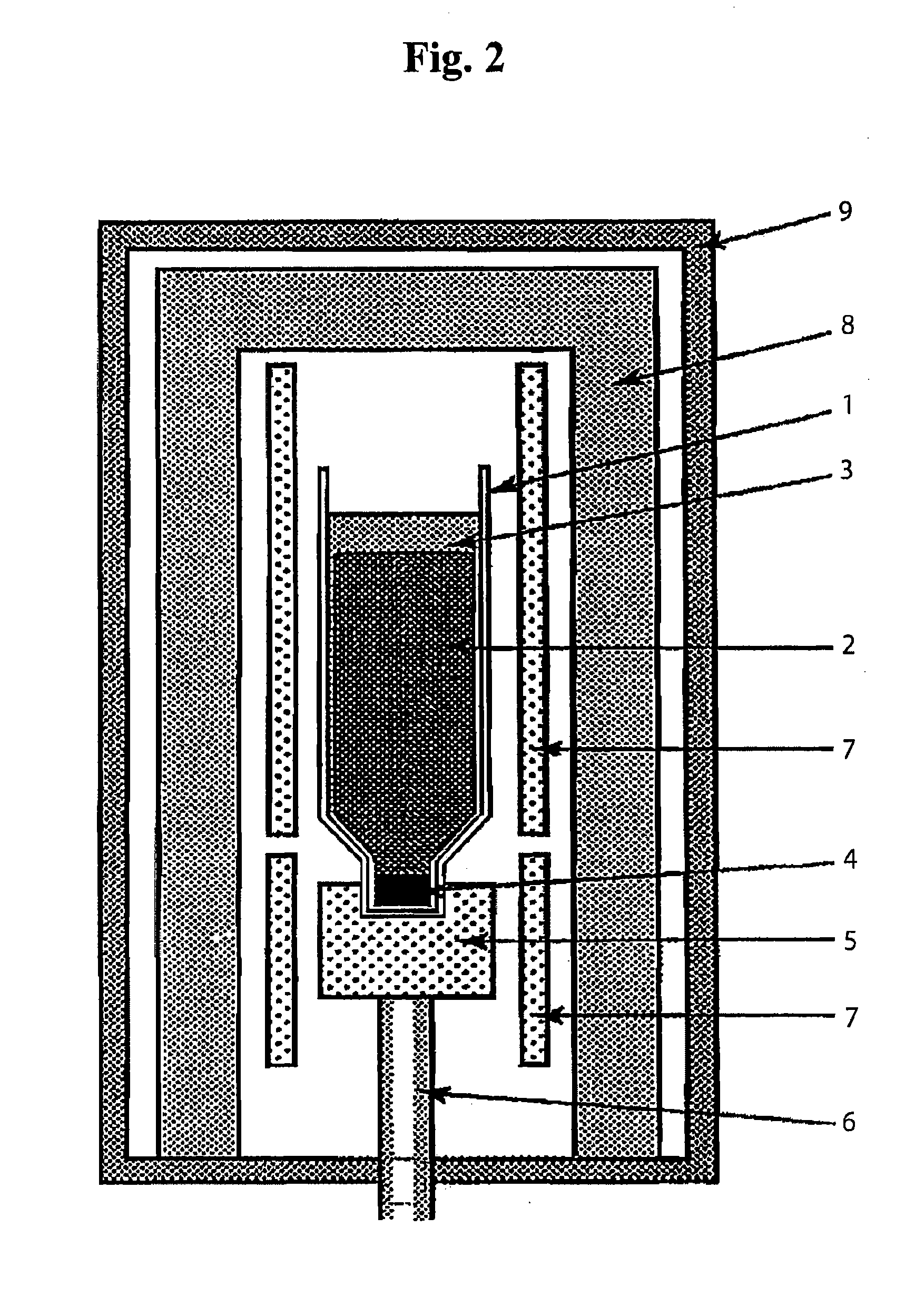
[0038]An InP seed crystal of 40 mm diameter and 40 mm length is placed in a pBN crucible 1 which has an inner diameter of approximately 105 mm and which has a boron oxide (B2O3) film on the inner surface. The cross-sectional area ratio of the seed crystal with respect to the crystal body is 15%. In addition, the tapered part from the seed crystal to the crystal body has a slope angle of 40 degrees with respect to the crystal central axis. The target value for the average dislocation density of the crystal to be grown is less than 5000 cm−2, and a seed crystal with an average dislocation density of 4500 cm−2 is used. For the dopant, high purity Fe is used, and this is housed in the pBN crucible together with 10 kg of InP polycrystal and 0.5 kg of boron oxide. The weight of high purity Fe placed in the crucible is adjusted so that the concentration at the front end of the straight body section is 2×1016 cm−3.

[0039]Crystal growth is seen in FIG. 2. For the growth of InP monocrystal, a...

embodiment 2

[0044]An InP seed crystal of 75 mm diameter and 30 mm length is placed in a pBN crucible 1 which has an inner diameter of approximately 105 mm and which has a boron oxide (B2O3) film on the inner surface. The cross-sectional area ratio of the seed crystal with respect to the crystal body is 50%. In addition, the tapered part from the seed crystal to the crystal body has a slope angle of 20 degrees with respect to the crystal central axis. The target value for the average dislocation density of the crystal to be grown is less than 3000 cm−2, and a seed crystal with an average dislocation density of 2500 cm−2 is used. For the dopant, high purity Fe is used, and this is housed in the pBN crucible together with 10 kg of InP polycrystal and 0.5 kg of boron oxide. The weight of high purity Fe placed in the crucible is adjusted so that the concentration at the front end of the straight body section is 2×1016 cm−3.

[0045]For the growth of InP monocrystal, a high pressure chamber 9 made of s...

embodiment 3

[0050]An InP seed crystal of 98 mm diameter and 20 mm length is placed in a pBN crucible 1 which has an inner diameter of approximately 105 mm and which has a boron oxide (B2O3) film on the inner surface. The cross-sectional area ratio of the seed crystal with respect to the crystal body is 87%. In addition, the tapered part from the seed crystal to the crystal body has a slope angle of 10 degrees with respect to the crystal central axis. The target value for the average dislocation density of the crystal to be grown is set at less than 2000 cm−2, and a seed crystal with an average dislocation density of 1500 cm−2 is used. For the dopant, high purity Fe is used, and this is housed in the pBN crucible together with 10 kg of InP polycrystal and 0.5 kg of boron oxide. The weight of high purity Fe placed in the crucible is adjusted so that the concentration at the front end of the straight body section of the crystal is 2×1016 cm−3.

[0051]For the growth of InP monocrystal, a high pressu...


PUM

PropertyMeasurementUnit
diameteraaaaaaaaaa
diameteraaaaaaaaaa
diameteraaaaaaaaaa

Abstract

An indium phosphide substrate for semiconductor devices is obtained as follows. In order to have the direction of growth of the crystal in the <100> orientation, a seed crystal having a specified cross-sectional area ratio with the crystal body is placed at the lower end of a growth container. The growth container housing the seed crystal, indium phosphide raw material, dopant, and boron oxide is placed in a crystal growth chamber. The temperature is raised to at or above the melting point of indium phosphide. After melting the boron oxide, indium phosphide raw material, and dopant, the temperature of the growth container is lowered in order to obtain an indium phosphide monocrystal. An average dislocation density is a function of a carrier density and diameter of the substrate, dislocation density, and a dopant concentration on the wafer is substantially uniform in the depth direction.

Description

CROSS-REFERENCE TO RELATED APPLICATIONS[0001]This application is a continuation-in-part of U.S. patent application Ser. No. 10 / 551,923, filed on Oct. 3, 2005, which is a national phase application of International Application No. PCT / JP2004 / 006427, file on May 6, 2004, claiming priority from Japanese Patent Application No. 2003-128831, filed on May 7, 2003, the disclosures of each of which being hereby incorporated by reference in its entirety herein. The International Application was published in Japanese on Dec. 9, 2004 as WO 2004 / 106597 A1 under PCT Article 21(2).TECHNICAL FIELD[0002]The present invention relates to an indium phosphide substrate, indium phosphide crystal, and method of manufacturing thereof used in the optoelectronics field such as semiconductor lasers for optical communication, photodetectors, and the like, and in the electronics field such as transistors and the like.BACKGROUND ART[0003]Indium phosphide (InP) crystals are manufactured by liquid encapsulated Czo...

Claims


Application Information

Patent Timeline
Patent Type & Authority Applications(United States)
IPC IPC(8): H01B1/02C30B17/00
CPCC30B29/40C30B11/00
Inventor KAWASE, TOMOHIRO
Owner SUMITOMO ELECTRIC IND LTD
Why Eureka
Try Eureka