Method of manufacturing semiconductor device

a manufacturing method and semiconductor technology, applied in the direction of semiconductor devices, basic electric elements, electrical appliances, etc., can solve the problems of reducing the reliability of semiconductor devices manufactured using soi substrates, reducing the electrical characteristics of transistors, and increasing threshold voltage and leakage current, so as to reduce reliability, suppress the amount of impurities entering the semiconductor film over the base substrate, and prevent the effect of impurities

Inactive Publication Date: 2009-04-16
SEMICON ENERGY LAB CO LTD
View PDF53 Cites 23 Cited by
  • Summary
  • Abstract
  • Description
  • Claims
  • Application Information

AI Technical Summary

Benefits of technology

[0015]In the present invention, after the formation of the fragile layer, a region on and near the surface of the insulating film where impurity contamination or adhesion of particles is remarkable is removed by etching, polishing, or the like. Therefore, the amount of impurities which enter the semiconductor film over the base substrate can be suppressed. In the semiconductor device which is completed finally with the use of the base substrate over which the semiconductor film is formed, it is possible to prevent the impurities from causing decrease in reliability and decrease in electrical characteristics of transistors, such as variation in threshold voltage or increase in leakage cu

Problems solved by technology

Despite the advantage of short takt time, the ion doping method has a risk that impurities such as a metal element included in a material of an electrode in an ion doping apparatus are introduced to the semiconductor substrate together with hydrogen ions because mass separation is not performed.
Since the above impurities are included in an SOI substrate to be completed finally, a semiconductor device

Method used


Image

  • Method of manufacturing semiconductor device
  • Method of manufacturing semiconductor device
  • Method of manufacturing semiconductor device

Examples


embodiment mode 1

[0034]In this embodiment mode, a method of manufacturing a semiconductor device of the present invention is described.

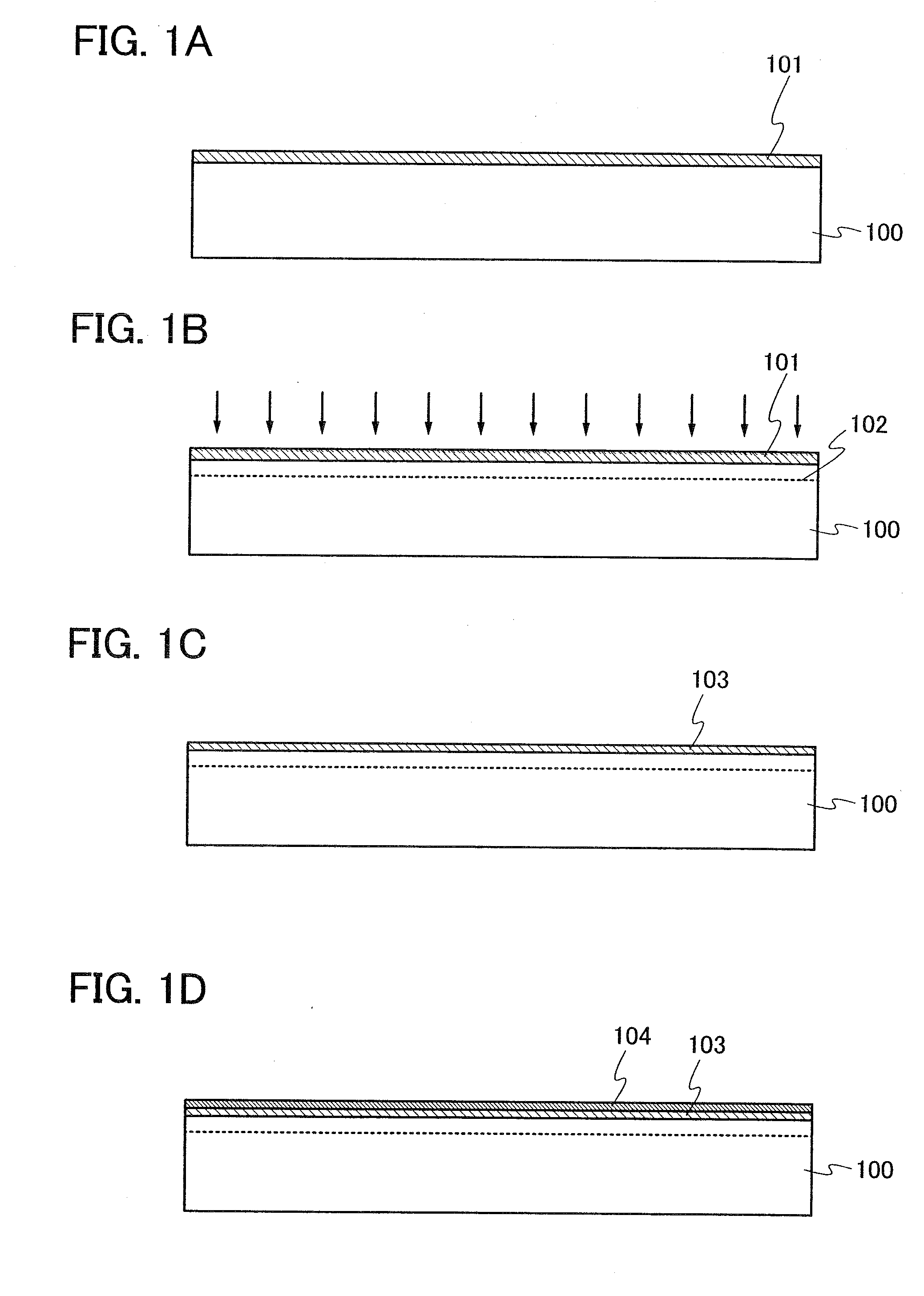
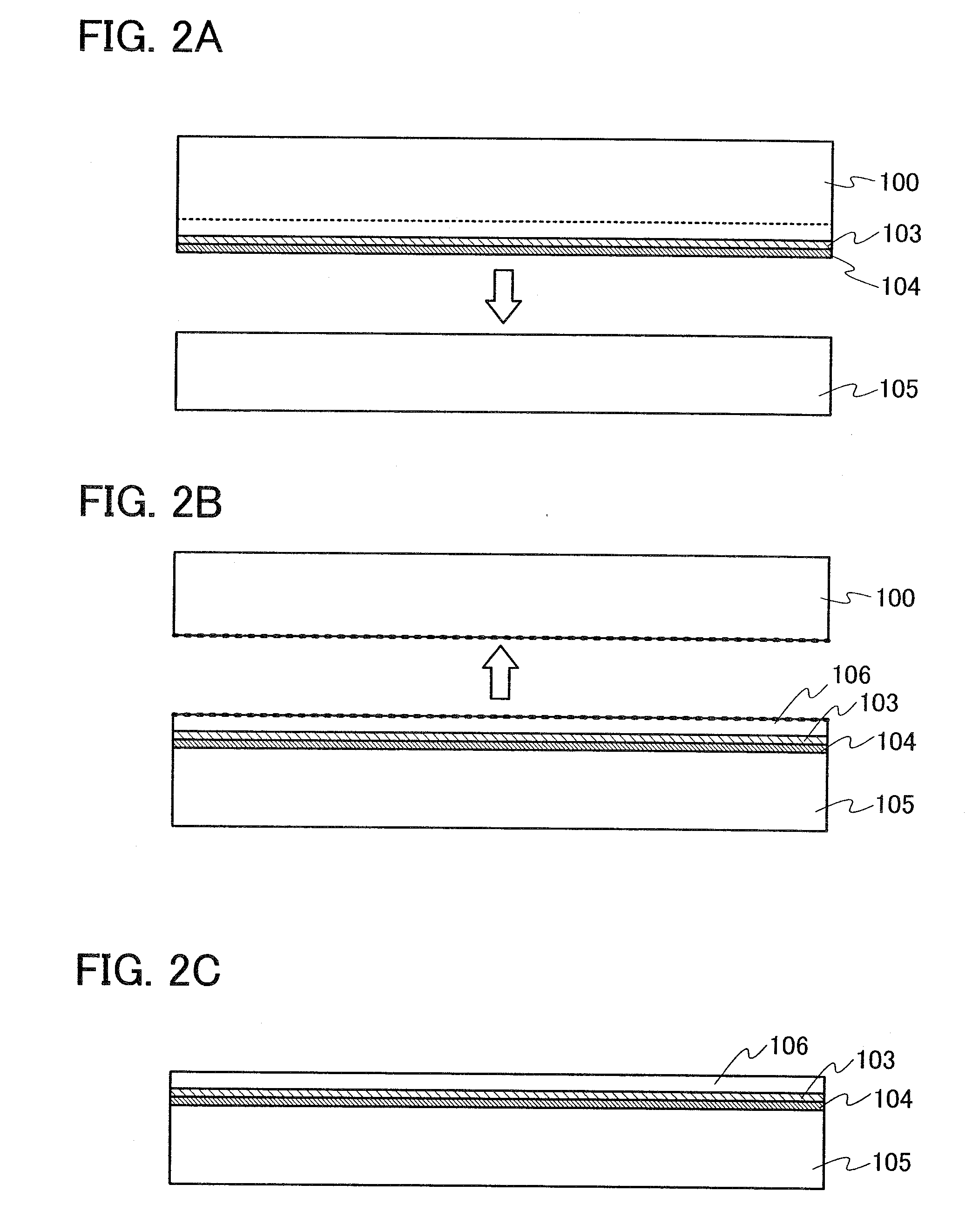
[0035]First, a bonding substrate 100 is cleaned and then an insulating film 101 is formed over the bonding substrate 100, as shown in FIG. 1A. As the bonding substrate 100, a single crystal or polycrystalline semiconductor substrate formed of silicon, germanium, or the like can be used. Alternatively, a single crystal or polycrystalline semiconductor substrate formed of a compound semiconductor such as gallium arsenide or indium phosphide can be used as the bonding substrate 100. Further alternatively, a semiconductor substrate formed of silicon having crystal lattice distortion, silicon germanium which is obtained by adding germanium to silicon, or the like may be used as the bonding substrate 100. Silicon having distortion can be formed by formation of silicon on silicon germanium or silicon nitride which has larger lattice constant than silicon.

[0036]The bonding s...

embodiment mode 2

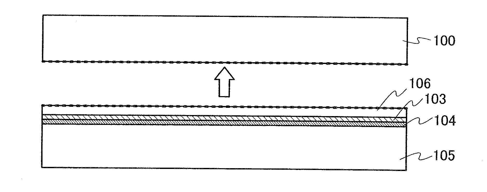
[0117]Unlike Embodiment Mode 1, this embodiment mode describes a method of manufacturing a semiconductor device of the present invention, in which the fragile layer 102 is formed before the formation of the insulating film 103.

[0118]First, after cleaning the bonding substrate 100, an ion beam including ions accelerated by an electric field is delivered to the bonding substrate 100 as indicated by arrows, whereby the fragile layer 102 having very small voids is formed in a region at a predetermined depth from a surface of the bonding substrate 100, as shown in FIG. 4A. The depth at which the fragile layer 102 is formed can be adjusted by the acceleration energy of the ion beam and the angle at which the ion beam enters. The acceleration energy can be adjusted by acceleration voltage, dosage, or the like. The fragile layer 102 can be formed at the same depth or substantially the same depth as the average depth at which the ions have entered. The thickness of the semiconductor film 106...

embodiment mode 3

[0146]This embodiment mode describes a method of manufacturing a thin film transistor, one of semiconductor elements, as an example of a method of manufacturing a semiconductor device with use of a base substrate with a semiconductor film attached, a so-called SOI substrate. A variety of semiconductor devices can be formed by combination of a plurality of thin film transistors.

[0147]First, the semiconductor film 106 over the base substrate 105 is processed (patterned) into a desired shape by etching, thereby forming semiconductor films 603 and 604 as shown in FIG. SA.

[0148]In order to control threshold voltage, a p-type impurity such as boron, aluminum, or gallium or an n-type impurity such as phosphorus or arsenic may be added to the semiconductor films 603 and 604. For example, in the case of adding boron as the p-type impurity, boron may be added at a concentration in the range of 5×10¹⁶ atoms / cm3 to 1×10¹⁷ atoms / cm3. The impurity for controlling the threshold voltage may be adde...


PUM


Abstract

To provide a method of manufacturing a semiconductor device, which prevents impurities from entering an SOI substrate. A source gas including one or plural kinds selected from a hydrogen gas, a helium gas, or halogen gas are excited to generate ions, and the ions are added to a bonding substrate to thereby form a fragile layer in the bonding substrate. Then, a region of the bonding substrate that is on and near the surface thereof, i.e., a region ranging from a shallower position than the fragile layer to the surface is removed by etching, polishing, or the like. Next, after attaching the bonding substrate to a base substrate, the bonding substrate is separated at the fragile layer to thereby form a semiconductor film over the base substrate. After forming the semiconductor film over the base substrate, a semiconductor element is formed using the semiconductor film.

Description

BACKGROUND OF THE INVENTION[0001]1. Field of the Invention[0002]The present invention relates to a method of manufacturing a semiconductor device with use of an SOI (silicon on insulator) substrate. The present invention particularly relates to a bonding SOI technique, and also to a method of manufacturing a semiconductor device with the use of an SOI substrate obtained by attaching a single crystal or polycrystalline semiconductor film to a substrate with an insulating film interposed between the semiconductor film and the substrate.[0003]2. Description of the Related Art[0004]Demands for higher integration, higher operation speed, higher performance, and lower power consumption have been more stringent, and in response to such demands, a transistor using an SOI substrate has attracted attention as an effective means that can take the place of a bulk transistor. Higher operation speed and lower power consumption can be expected more in the transistor using the SOI substrate than in...

Claims


Application Information

Patent Timeline
IPC IPC(8): H01L21/762
CPCH01L21/76254H01L29/66772H01L27/1266H01L27/1214H01L27/12
Inventor OHNUMA, HIDETOIIKUBO, YOICHIYAMAZAKI, SHUNPEI
Owner SEMICON ENERGY LAB CO LTD
Why Eureka
Try Eureka