

Method for manufacturing semiconductor device, and semiconductor device and electronic device
- Summary
- Abstract
- Description
- Claims
- Application Information
AI Technical Summary
Benefits of technology
Problems solved by technology
Method used
Image

Examples
embodiment mode 1
[0060]In this embodiment mode, an example of a method for manufacturing a semiconductor device of the present invention will be described.
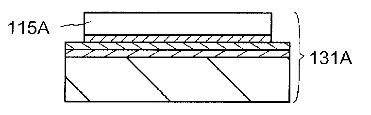
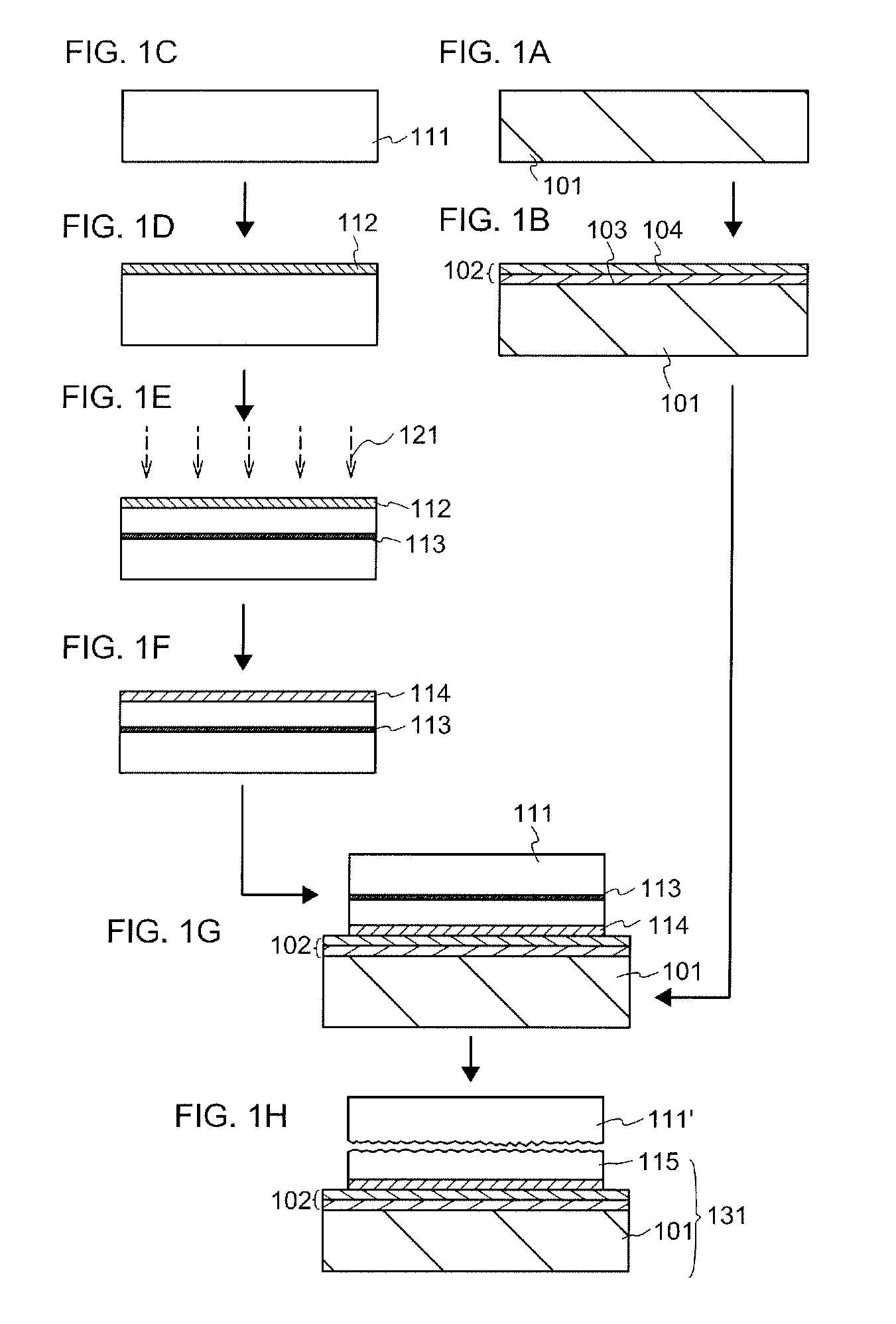
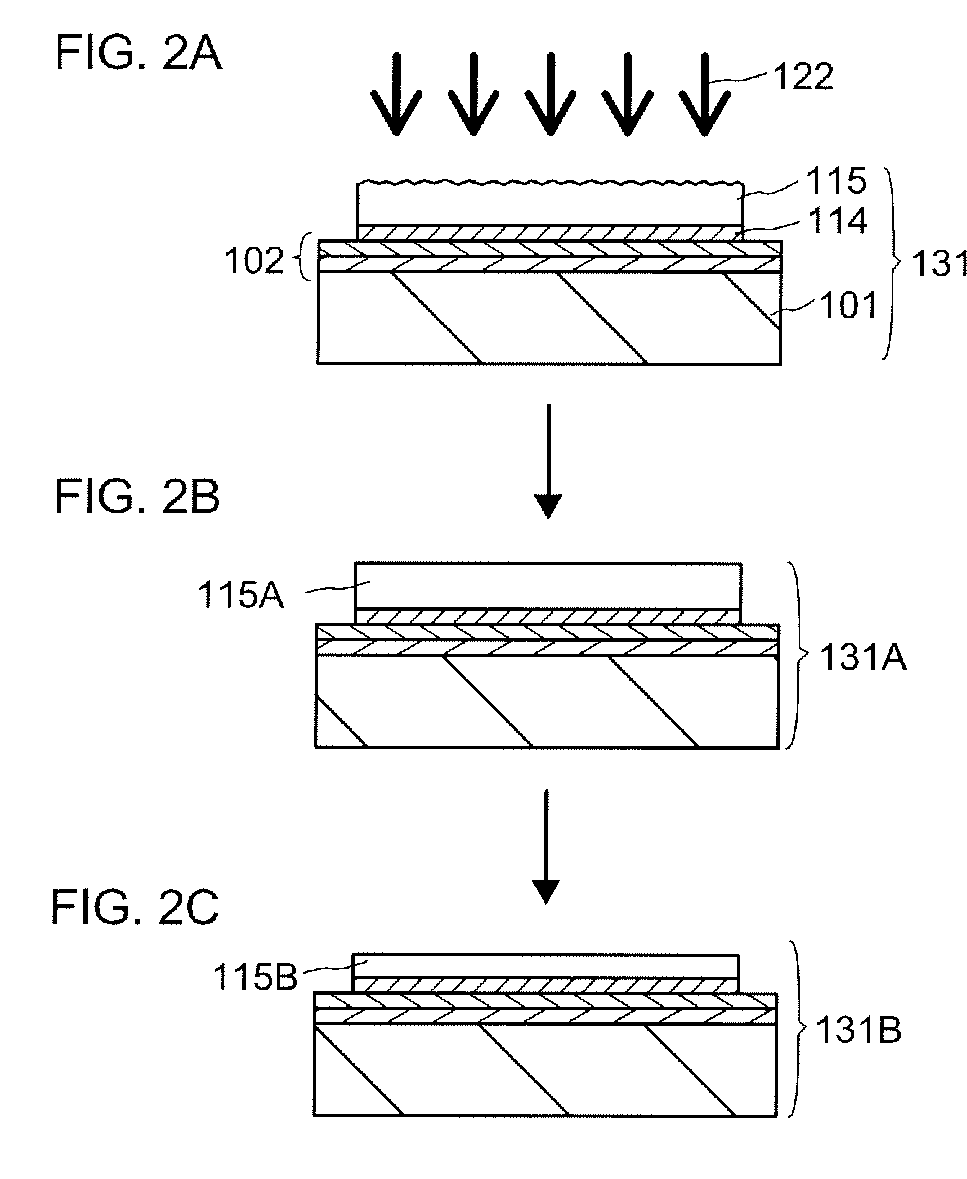
[0061]First, a method for manufacturing an SOI substrate which is used for a semiconductor device will be described with reference to FIGS. 1A to 1H, FIGS. 2A to 2C, and FIGS. 3A to 3C.
[0062]First, a base substrate 101 is prepared (see FIG. 1A). As the base substrate 101, a light-transmitting glass substrate used for the products of electronics industry such as a liquid crystal display device can be used. A substrate having a strain point greater than or equal to 580° C. (preferably greater than or equal to 600° C.) may be used as the glass substrate. Further, the glass substrate is preferably a non-alkali glass substrate. As a material of the non-alkali glass substrate, a glass material such as aluminosilicate glass, aluminoborosilicate glass, or barium borosilicate glass is used, for example.
[0063]Note that as the base substrate 101, as well as ...
embodiment mode 2
[0221]In this embodiment mode, another example of a method for manufacturing an SOI substrate will be described with reference to FIGS. 7A to 7G and FIGS. 8A to 8C.
[0222]The base substrate 101 to be a base substrate of an SOI substrate is prepared in a manner similar to that of Embodiment Mode 1 (see FIG. 7A). FIG. 7A is a cross-sectional view of the base substrate 101. The semiconductor substrate 111 is prepared (see FIG. 7B). FIG. 7B is a cross-sectional view of the semiconductor substrate 111.
[0223]After the semiconductor substrate 111 is washed, an insulating layer 116 is formed on the surface of the semiconductor substrate 111 (see FIG. 7C). The insulating layer 116 can have a single-layer structure or a multilayer structure of two or more layers. The thickness of the insulating layer 116 can be greater than or equal to 10 nm and less than or equal to 400 nm.
[0224]As a film which forms the insulating layer 116, an insulating film containing silicon or germanium as its component...
embodiment mode 3
[0245]In this embodiment mode, another example of a method for manufacturing an SOI substrate will be described with reference to FIGS. 9A to 9H and FIGS. 10A to 10C.
[0246]The base substrate 101 to be a base substrate of an SOI substrate is prepared in a manner similar to that of Embodiment Mode 1 (see FIG. 9A), and the insulating layer 102 is formed over the base substrate. Also in this embodiment, the insulating layer 102 is a film with a two-layer structure including the silicon nitride oxide film 103 and the silicon oxynitride film 104. Next, a bonding layer 105 is formed over the insulating layer 102 (see FIG. 9B). This bonding layer 105 can be formed similarly to the bonding layer 114 formed over the semiconductor substrate 111 which is shown in Embodiment Mode 1 or 2.
[0247]FIGS. 9C to 9E shows steps similar to those in FIGS. 1C to 1E. As described in Embodiment Mode 1, the protective film 112 is formed over the semiconductor substrate 111, and the damaged region 113 is formed...
PUM
 Abstract
Description
Claims
Application Information