

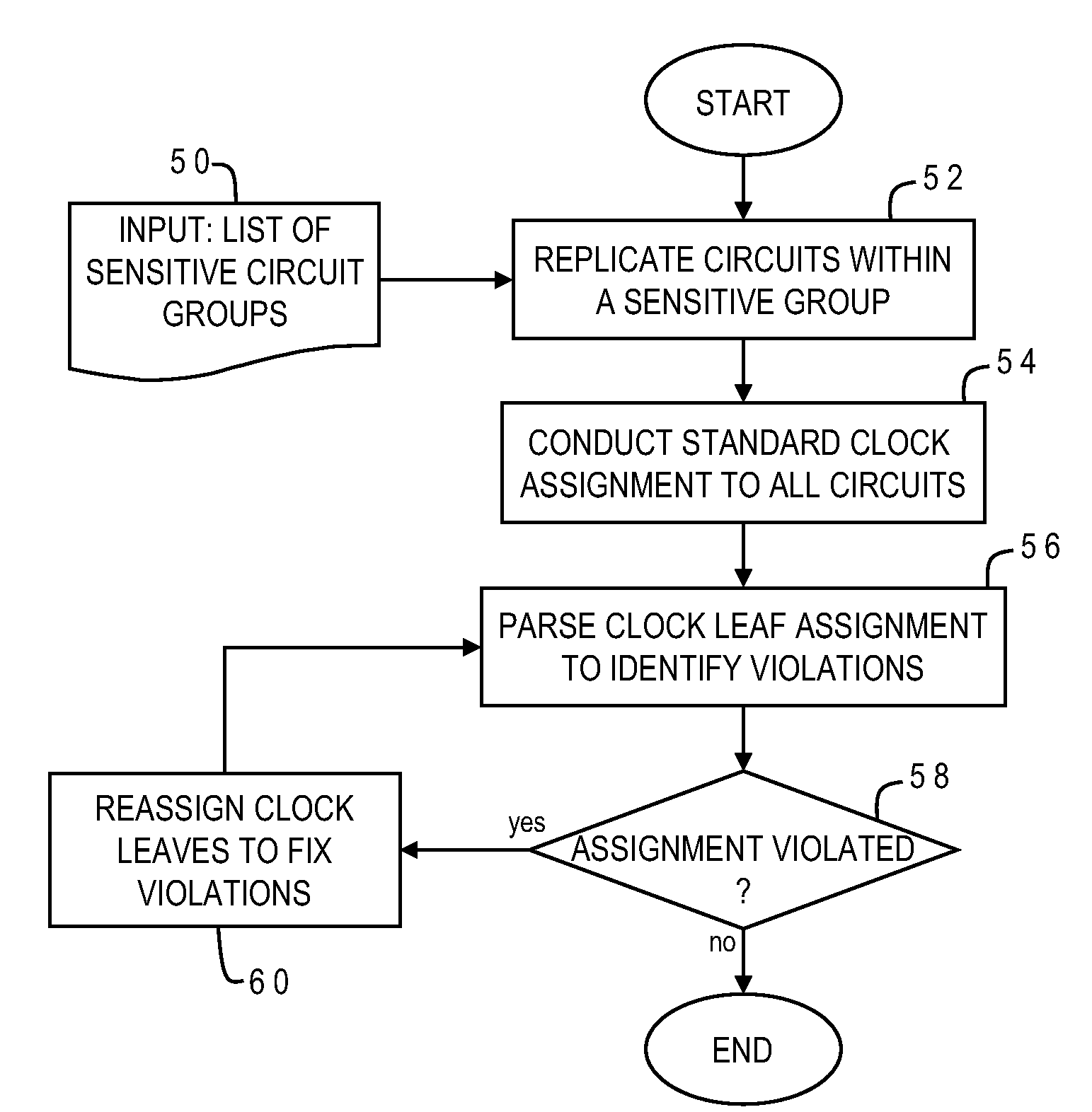
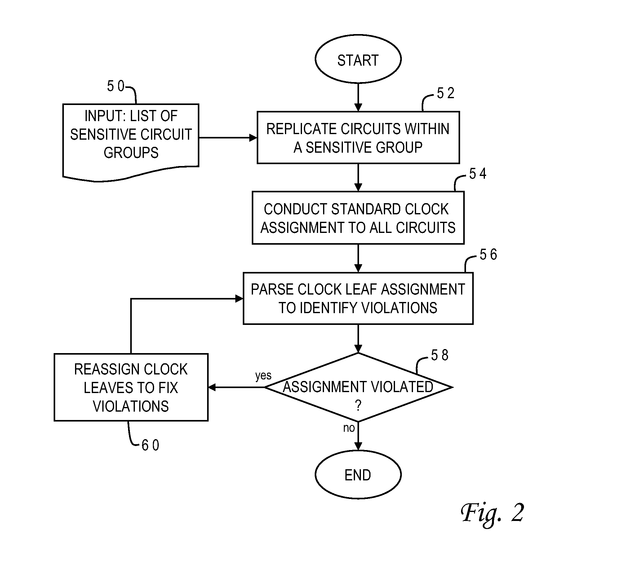
Radiation Tolerance by Clock Signal Interleaving
a clock signal and clock signal technology, applied in the field of fabrication and design of semiconductor chips and integrated circuits, can solve the problems of large number of cells, difficult computer-aided design, and complicated connections between cells, and achieve the effect of increasing radiation toleran
- Summary
- Abstract
- Description
- Claims
- Application Information
AI Technical Summary
Benefits of technology
Problems solved by technology
Method used
Image

Examples
Embodiment Construction
)
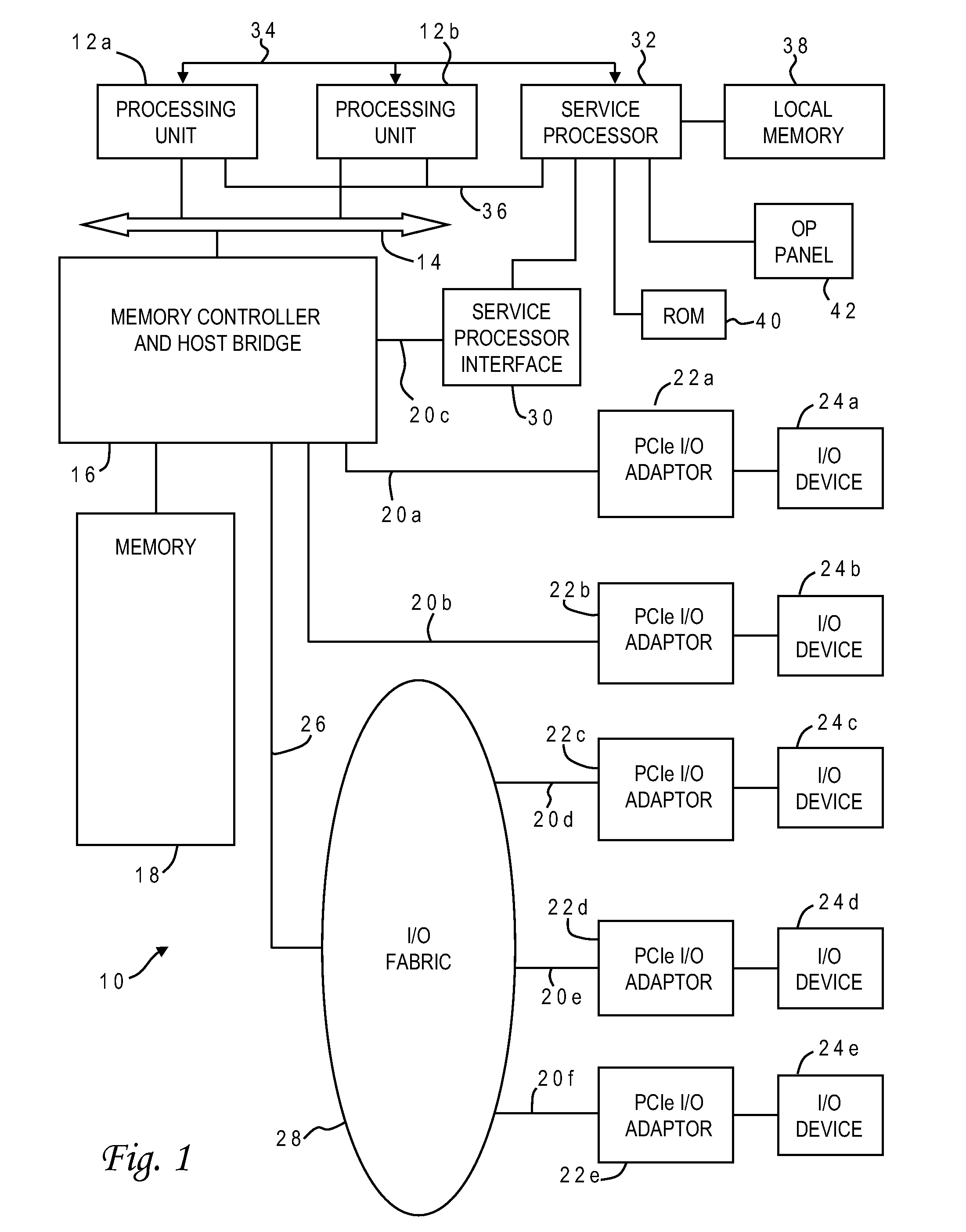
[0026]With reference now to the figures, and in particular with reference to FIG. 1, there is depicted one embodiment 10 of a computer system in which the present invention may be implemented to carry out the design of logic structures in an integrated circuit. Computer system 10 is a symmetric multiprocessor (SMP) system having a plurality of processors 12a, 12b connected to a system bus 14. System bus 14 is further connected to a combined memory controller / host bridge (MC / HB) 16 which provides an interface to system memory 18. System memory 18 may be a local memory device or alternatively may include a plurality of distributed memory devices, preferably dynamic random-access memory (DRAM). There may be additional structures in the memory hierarchy which are not depicted, such as on-board (L1) and second-level (L2) or third-level (L3) caches.
[0027]MC / HB 16 also has an interface to peripheral component interconnect (PCI) Express links 20a, 20b, 20c. Each PCI Express (PCIe) link 20a...
PUM
 Abstract
Description
Claims
Application Information