Method for modifying high-k dielectric thin film and semiconductor device

a technology of dielectric thin film and semiconductor device, which is applied in the direction of semiconductor device, semiconductor/solid-state device details, electrical apparatus, etc., can solve the problems of increasing gate leakage current, unstable critical value of transistor, and carrier scattering problem in channel region, so as to prevent deficiency occurrence, improve electrical characteristics, and film density increase

Inactive Publication Date: 2009-12-10
TOKYO ELECTRON LTD
View PDF5 Cites 4 Cited by
  • Summary
  • Abstract
  • Description
  • Claims
  • Application Information

AI Technical Summary

Benefits of technology

[0013]In view of the above, the present invention provides a method for modifying a high-k dielectric thin film and a semiconductor device capable of increasing a dielectric constant and achieving better electrical characteristics by preventing deficiency and increasing the film density by removing carbon components in the high-k dielectric thin film and sintering the film by means of applying ultraviolet rays to the high-k dielectric thin film at a predetermined temperature in an inert gas atmosphere or in an oxygen atmosphere.

Problems solved by technology

However, in such an extremely thin gate insulating film, a tunneling current is increased, which in turn increases a gate leakage current.
In case of a gate insulating film formed by coating a high-k dielectric thin film directly on a silicon substrate or film, metal elements in the high-k dielectric film tend to diffuse into the silicon substrate or film to thereby cause a carrier scattering problem in a channel region.
Therefore, the included carbon components reduce a dielectric constant to cause a leakage current and further make a critical value of the transistor unstable.
However, since removal of the carbon components by high temperature annealing reduces the film density, the dielectric constant is reduced, which deteriorates film quality and cannot provide desired electrical characteristics.
However, in the method for exposing a high-k dielectric thin film to plasma-excited oxygen radicals, uncontrolled excessive radicals are formed and they pass through the high-k dielectric thin film to increase the thickness of the SiO2 film serving as a base film, resulting in an increase of the Equivalent Oxide Thickness (EOT) of the gate insulating film.
Further, since the UV-O3 processing method described above uses ozone which is a strong oxidizing agent, the thickness of the SiO2 film serving as a base film increases at the same time as the oxygen deficiency is compensated for, which results in an increase in the EOT of the gate insulating film.

Method used


Image

  • Method for modifying high-k dielectric thin film and semiconductor device
  • Method for modifying high-k dielectric thin film and semiconductor device
  • Method for modifying high-k dielectric thin film and semiconductor device

Examples


first embodiment

[0082]The method in accordance with the first embodiment of the present invention will be described.

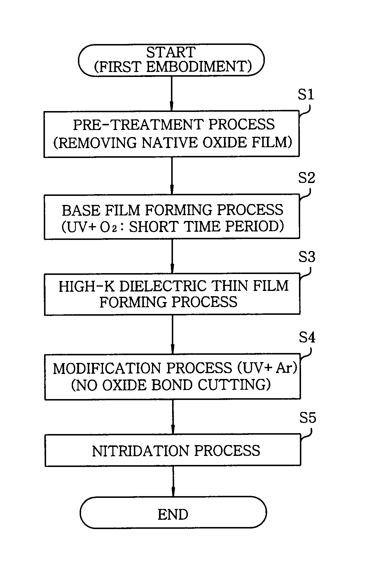
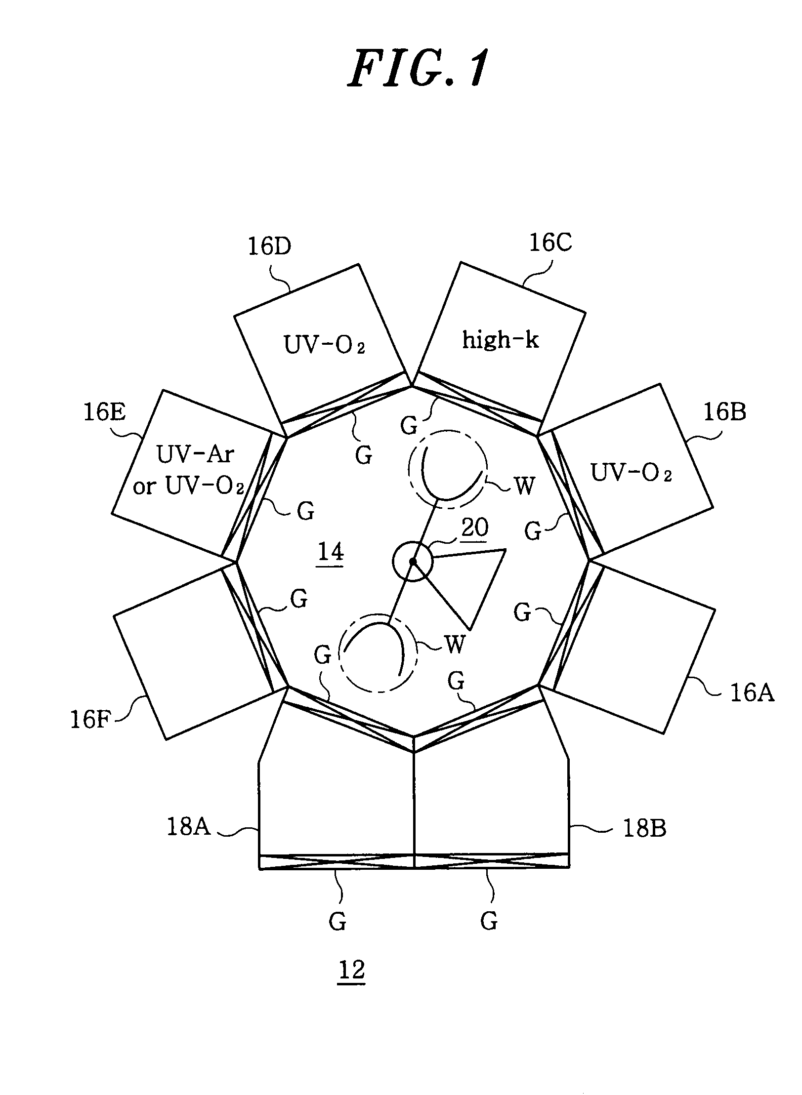
[0083]FIG. 3 is a flow chart illustrating the process of the method of the first embodiment. First, a semiconductor wafer W to be processed is loaded into the common transfer chamber 14 through the load-lock chamber 18A or 18B (see FIG. 1) and then transferred to the pretreatment apparatus 16A to be pretreated (step S1). In the pretreatment process, a native oxide film on the surface of the wafer W is removed by using nitrogen radicals, oxygen radicals and NF gases as described above.

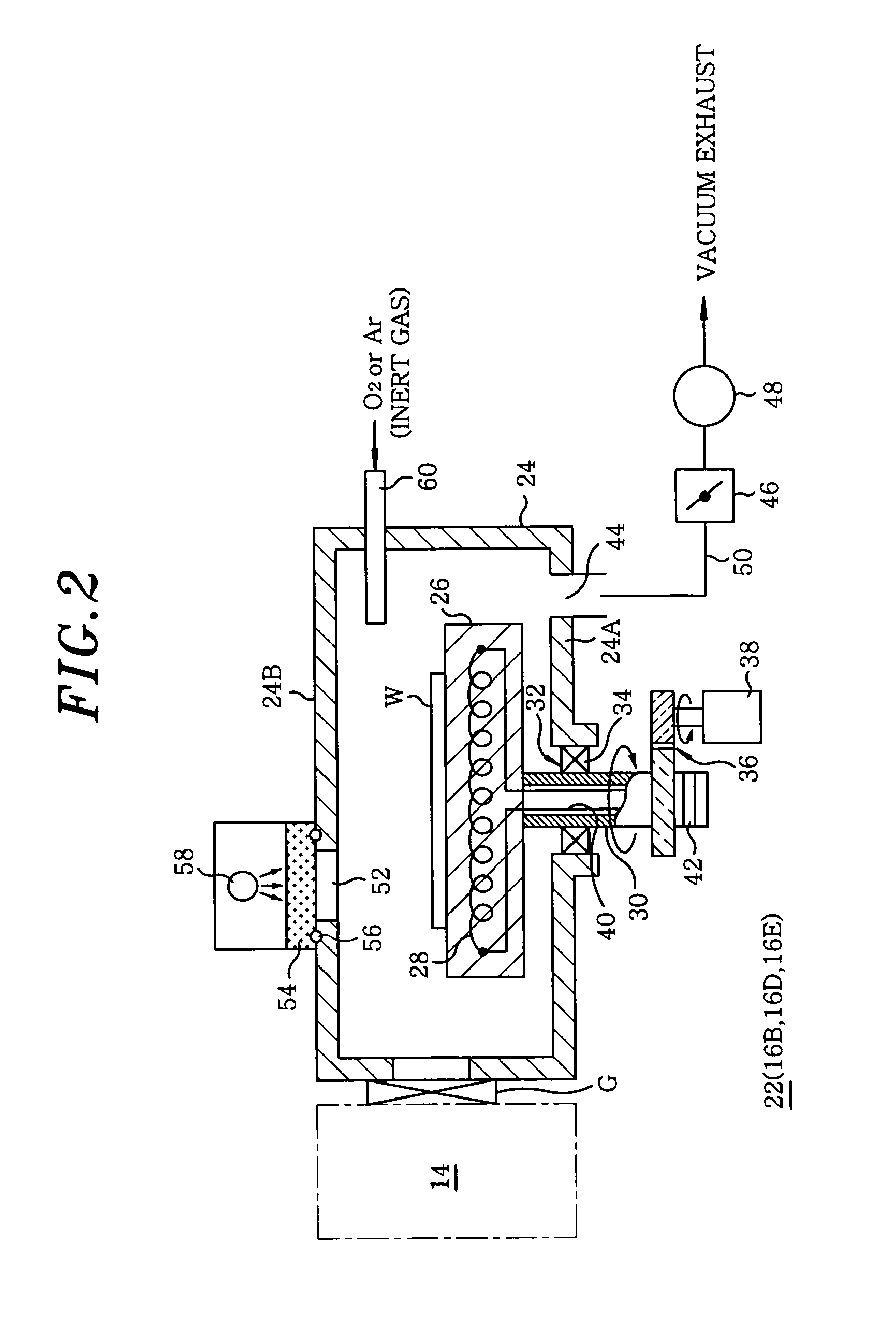
[0084]When the pretreatment process is completed, the wafer W is transferred from the pretreatment apparatus 16A to the base film forming apparatus 16B and a base film forming process is conducted (step S2). The base film forming apparatus 16B has the structure shown in FIG. 2. A base film 2 (see FIG. 15) which is a very thin SiO2 film of high surface uniformity is formed by oxidizing the surface of the w...

second embodiment

[0107]Hereinafter, a method in accordance with the second embodiment of the present invention will be described.

[0108]FIG. 5 is a flow chart illustrating a process of the method of the second embodiment. The second embodiment is different from the first embodiment described in FIG. 3 in that a reoxidation process of the step S3-1 is provided between the steps S3 and S4 in FIG. 3. In this case, modification operations are performed in both the reoxidation process of the step S3-1 and the modification process of the step S4.

[0109]To be specific, when the high-k dielectric thin film forming process of the step S3 is completed, the wafer W is transferred from the CVD processing apparatus 16C to the reoxidation apparatus 16D (see FIG. 1) and the reoxidation process of the present invention is then performed (step S3-1).

[0110]The reoxidation apparatus 16D has the structure shown in FIG. 2. UV rays from the UV lamp 58 are applied to the surface of the rotating wafer W mounted on the mounti...

third embodiment

[0118]Hereinafter, a method in accordance with the third embodiment of the present invention will be described.

[0119]FIG. 6 is a flow chart illustrating a process of the method of the third embodiment.

[0120]In the third embodiment, the order of the reoxidation process of the step S3-1 and modification process of the step S4 of the second embodiment shown in FIG. 5 are reversed and the reoxidation process is indicated here as the step S4-1.

[0121]The third embodiment can provide the same effects as those in the first embodiment as described above. Further, in the third embodiment, the film quality is improved by compensating for the oxygen deficiency of the high-k dielectric thin film 4 and the film density is increased by reducing the carbon concentration and sintering, as described in the second embodiment.

[0122]If UV rays are applied to the high-k dielectric thin film 4 in an Ar atmosphere in the modification process of the step S4, the film surface may be damaged by UV rays with h...


PUM

PropertyMeasurementUnit
wavelengthaaaaaaaaaa
temperatureaaaaaaaaaa
thicknessaaaaaaaaaa

Abstract

There is provided a method for modifying a high-k dielectric thin film provided on the surface of an object using a metal organic compound material. The method includes a preparation process for providing the object with the high-k dielectric thin film formed on the surface thereof, and a modification process for applying UV rays to the highly dielectric thin film in an inert gas atmosphere while maintaining the object at a predetermined temperature to modify the high-k dielectric thin film. According to the above constitution, the carbon component can be eliminated from the high-k dielectric thin film, and the whole material can be thermally shrunk to improve the density, whereby the occurrence of defects can be prevented and the film density can be improved to enhance the specific permittivity and thus to provide a high level of electric properties.

Description

FIELD OF THE INVENTION[0001]The present invention relates to a method for modifying a high-k dielectric thin film formed on a target object such as a semiconductor wafer and the like, and a semiconductor device using a gate insulating film obtained by the modification.BACKGROUND OF THE INVENTION[0002]In general, in a manufacturing process of a semiconductor integrated circuit, various single-substrate processes such as a film forming process, an etching process, a heat treatment process, a modification process and a crystallization process are repeated on a target object such as a semiconductor wafer to form the desired integrated circuit.[0003]With the recent trend of thin-film integrated circuits featuring a high operation speed and high integration, the line width and film thickness of the integrated circuit become smaller. For example, in case of a semiconductor device of a semiconductor integrated circuit, e.g. a transistor, it is required to further reduce the width of the gat...

Claims


Application Information

Patent Timeline
Patent Type & Authority Applications(United States)
IPC IPC(8): H01L21/3105H01L21/316H01L21/268H01L29/78
CPCH01L21/268H01L21/28211H01L21/67207H01L21/318H01L21/31645H01L21/02211H01L21/02271H01L21/02148H01L21/02181H01L21/02329H01L21/02164H01L21/0234H01L21/02348
Inventor YAMAZAKI, KAZUYOSHIAOYAMA, SHINTAROAKIYAMA, KOJI
Owner TOKYO ELECTRON LTD
Why Eureka
Try Eureka