

Light emitting device and light emitting apparatus
- Summary
- Abstract
- Description
- Claims
- Application Information
AI Technical Summary
Benefits of technology
Problems solved by technology
Method used
Image

Examples
first embodiment
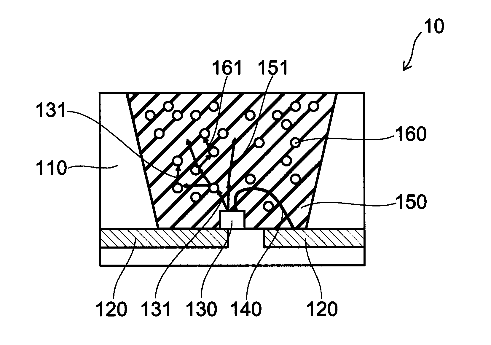
[0034]FIG. 1 is a schematic cross-sectional view illustrating the configuration of a light emitting device according to a first embodiment of the invention.
[0035]In the light emitting device 10 according to the first embodiment of the invention illustrated in FIG. 1, a package 110 contains a light source 130 and fluorescent materials. An electrode unit 120 is provided in the package 110 to provide a current to the light source 130. Wiring 140 is provided to connect the light source 130 and the electrode unit 120.
[0036]The fluorescent materials include a first fluorescent material (first wavelength conversion unit) 150 and a second fluorescent material (second wavelength conversion unit) 160. The second fluorescent material 160 is multiply dispersed in the first fluorescent material 150. In other words, the first fluorescent material 150 exists around the dispersed second fluorescent material 160.
[0037]The second fluorescent material 160 has a higher absorptance than the first fluore...
second embodiment
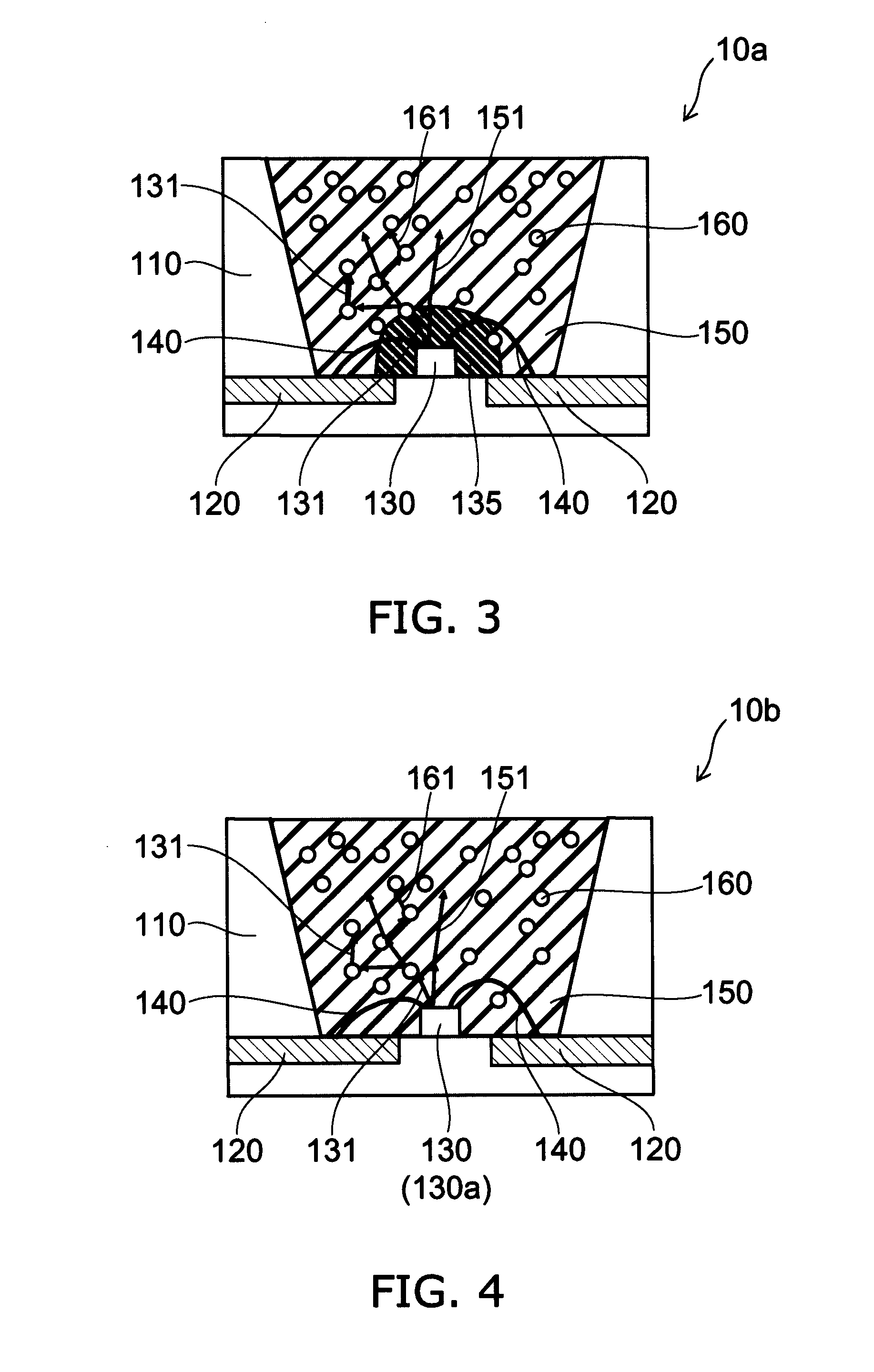
[0137]FIG. 5 is a schematic cross-sectional view illustrating the configuration of a light emitting device according to a second embodiment of the invention.
[0138]In the light emitting device 12 according to the second embodiment of the invention illustrated in FIG. 5, the concentration of the second fluorescent material (the second wavelength conversion unit) 160 in the first fluorescent material (the first wavelength conversion unit) 150 is higher on the side distal to the light source 130 than on the side proximal thereto. Otherwise, the light emitting device 12 may be similar to the light emitting device 10 according to the first embodiment, and a description is omitted.
[0139]In other words, the second fluorescent material 160 is disposed at a position in the interior of the first fluorescent material 150 distal to the light source 130. In the case where the concentration of the second fluorescent material 160, which has a high absorptance, is high proximal to the light source 1...
third embodiment
[0159]FIG. 7 is a schematic cross-sectional view illustrating the configuration of a light emitting device according to a third embodiment of the invention.
[0160]The light emitting device 13 according to the third embodiment of the invention illustrated in FIG. 7 further includes a moisture resisting cover 260 provided on the side of the first fluorescent material 150 opposite to the light source 130 to protect at least one of the first fluorescent material 150 and the second fluorescent material 160 against moisture.
[0161]In other words, the light emitting device 13 of this specific example is the light emitting device 10 described in the first embodiment having the moisture resisting cover 260 further provided thereon. Otherwise, the light emitting device 13 may be similar to the light emitting device 10 described in the first embodiment, and a description is omitted. Additionally, the moisture resisting cover 260 may be provided on the light emitting device 10a according to the f...
PUM
 Abstract
Description
Claims
Application Information