Silicate base luminescent materials having multiple emission peaks, processes for preparing the same and light emitting devices using the same

a luminescent material and silicate base technology, applied in the field of photoelectron and semiconductor lighting, can solve the problems of low color rendering index of white light led, large restriction of the application and performance of fluorescent materials used in this method, and affecting the performance of white light leds, etc., to achieve excellent ageing resistance and high light conversion efficiency

Active Publication Date: 2010-03-04
DALIAN LUMINGLIGHT SCIENCE & TECHNOLOGY CO LTD
View PDF10 Cites 17 Cited by
  • Summary
  • Abstract
  • Description
  • Claims
  • Application Information

AI Technical Summary

Benefits of technology

[0008]An object of the present invention is to provide a silicate luminescent material characterized by a broad excitation spectrum and multiple emission peaks, which has a broad excitation wavelength range (from 240 to 475 nm), at least two emission peaks in the wavelength range of from 370 to 760 nm, a high light conversion efficiency, and excellent ageing resistance. Another object of the present invention is to provide a process for producing such a silicate luminescent material. A third object of the present invention is to provide a light emitting device comprising the silicate luminescent material according to the invention, in particular a white light LED.
[0016]In the present invention, the broad excitation peak and emission peak wavelength ranges of the luminescent material are achieved by finely adjusting the amounts and combination of the metal elements A and / or A′ in the silicate luminescent material. The characteristics of transition between energy levels of a rare earth ion remarkably depend on its crystal structure, and this is utilized to adjust the absorption or emission wavelength of the rare earth ion to thereby generate light of different colors. In the present invention, the crystal field environment surrounding the used Eu and Ln ions in the crystal exerts a remarkable influence on 5d energy state and 4f-5d transition of these ions, so that the maximum absorption of the transition and the position of the emission peak remarkably vary as the crystal lattice environment of the substrate changes, and the emission wavelength may be finely adjusted in a range of from UV light to red light region. Moreover, by finely adjusting the amounts and combination of the metal elements A and / or A′ in the silicate luminescent material, for some allomeric compounds, the position of the emission peak may shift to longer wavelength or shorter wavelength regularly as the chemical composition of the substrate changes. In the present invention, by using charge transfer (CTS) transition, i.e., transfer of an electron from a fully occupied molecular orbit of a ligand (oxygen, M, etc.) to partially occupied 4f shell layer of a rare earth ion, a relatively broad charge transfer spectrum is achieved, so that the position of a band varies as the environment changes.
[0019]The incorporation of M and N is an important discovery and innovation in the present invention. The incorporation of M can remarkably broaden the excitation spectrum range of the luminescent material and enhance the excitation band adaptability of the luminescent material, and particularly can remarkably increase the strength of the red-side emission band of the luminescent material Eu2+. The incorporation of N may cause the crystal lattice environments surrounding the Eu2+ ions in different substrates markedly different from each other due to that the ionic radii of alkali metals are far lower than the ionic radii of alkaline earth metals. When Eu2+ enters a crystal lattice by substituting for an alkali metal ion, the distance between Eu2+ and O2− therein is less than the distance between Eu2+ and O2− in an alkaline earth metal substrate, so that the 5d energy of Eu2+ increases, i.e., the energy difference between the lowest 5d energy level of Eu2+ and its ground level becomes greater, and the luminescent intensity of the luminescent material is increased. The incorporation of Ag+ can also markedly increase the luminescent intensity of the luminescent material, but it has a different luminescence-enhancing effect than an alkali metal ion. Meanwhile, the incorporation of N has further the effect of charge compensation.
[0029]In order to improve the quality of the material, a minor amount (not exceeding 30% by weight of the raw materials) of other compounds, such as NH4Cl, NH4F, (NH4)2HPO4, glucose, urea, BaF2, CaF2, ZnF2, ZnS, SrS, CaS, SrSO4, SrHPO4, CaHPO4, Li2CO3, KNO3 or Na2CO3, may be added into the raw materials to participate in the solid phase reaction.
[0037]In a light emitting device according to a preferred embodiment of the invention, the light emitting element as the excitation light source has an emission spectrum having a peak value in a UV light to blue light range, and at least two light beams including at least a portion of light from the silicate luminescent material of the present invention and light from the second and / or the third and / or the fourth luminescent material are compounded, to thereby form white light.

Problems solved by technology

However, these methods are somewhat restricted due to the limitation of the fluorescent material.
The fluorescent materials used in this method apply great restriction to the application and performance of white light LEDs.
Secondly, the emission spectra of such fluorescent material powders of the rare earth garnet structure can only reach about 540 nm at the maximum and lack red light component, thereby resulting in a relatively low color rendering index of the white light LED.
The effective excitation wavelength range of such fluorescent materials is somewhat widened, and emission range can cover from green light to red light, but the luminance of these fluorescent materials is relatively low, and the production cost thereof is relatively high.
Thus, there is still great limitation to use these fluorescent materials as commercial LED phosphors.
However, the luminance of the sulfide fluorescent material is low so that it reduces the luminous efficiency of LED, although it increases the color rendering index.
Moreover, said fluorescent material has poor chemical stability and ageing resistance and corrodes a chip, thereby shortening the service lifetime of the LED.
In particular, the use of several phosphors has a very high requirement on the consistency in application properties, such as chemical stability, luminescent property and ageing property, of different kinds of the phosphors, and the handling of the phosphors in a preparation in packaging industry is strictly restricted.

Method used


Image

  • Silicate base luminescent materials having multiple emission peaks, processes for preparing the same and light emitting devices using the same
  • Silicate base luminescent materials having multiple emission peaks, processes for preparing the same and light emitting devices using the same
  • Silicate base luminescent materials having multiple emission peaks, processes for preparing the same and light emitting devices using the same

Examples


example 1

[0049]

Raw materialsWeight (g)BaCO3586.10MgO41.11SiO2120.78Eu2O31.76Mn3O43.81NH4F0.19Li2CO30.18

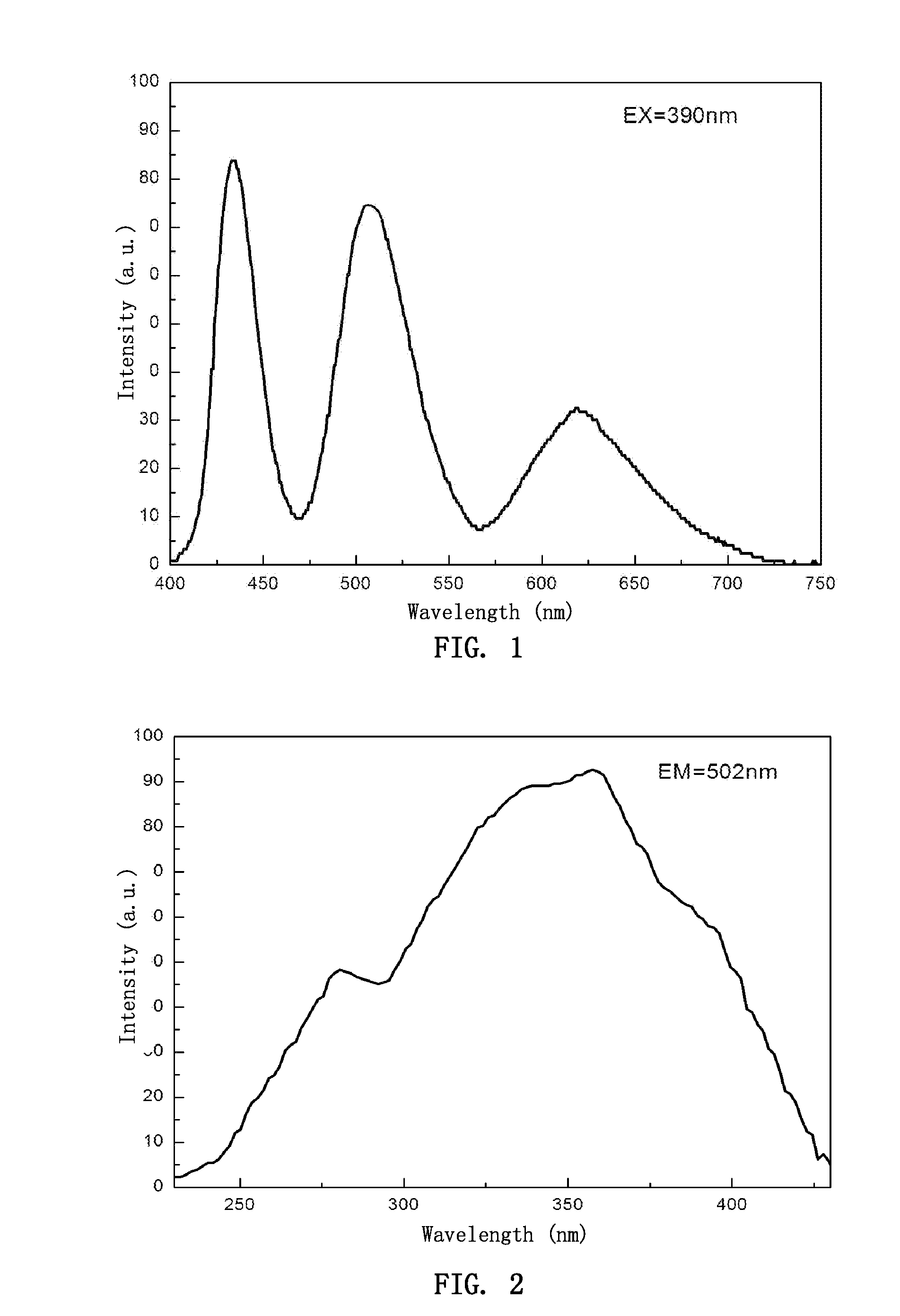
[0050]The raw materials according to the above composition were sufficiently mixed by a ball mill and then placed in a crucible. After cooling, the mixture was sintered in a furnace, through which a mixed gas consisting of 95% nitrogen and 5% hydrogen was passed, at 1200° C. for 6 hours. After cooling, the resultant sintered body was crushed, milled with a ball mill, and then sieved through a 325 mesh sieve, to give a luminescent material of the invention having a chemical composition of 2.97BaO.1.02MgO.2.01SiO2:0.01 Eu2+.0.05 Mn2+.0.005F−.0.005 Li+. The material had an excitation spectrum in the range of from 240 to 450 nm, and an emission spectrum in the range of from 400 to 760 nm with three emission peaks, of which peak wavelengths were at 438 nm, 502 nm and 617 nm, respectively.

examples 2 to 36

[0051]Luminescent materials of Examples 2 to 36 were prepared following the procedure described in Example 1, with the kinds and amounts of the elements A and A′ in the substrate composition being changed according to desired positions of emission peaks. The sintering temperature varied in the range of from 1000 to 1300° C. depending on the volume of the furnace, the weight of the materials, and the kind and formulation of the materials. The reducing atmosphere was provided by hydrogen gas, ammonia gas, a mixture of nitrogen and hydrogen, or a particulate carbon. Luminescent materials having two emission peaks with the following chemical compositions were obtained:

example 2

2.03SrO.0.92MgO.1.0SiO2:0.03Eu2+.0.02F−.0.07Li+


PUM

PropertyMeasurementUnit
wavelengthaaaaaaaaaa
temperatureaaaaaaaaaa
wavelength rangeaaaaaaaaaa

Abstract

A silicate luminescent material excitable by an excitation light source having emissions in UV to blue light region, a process for producing the same, and a white light emitting device. The luminescent material has an emission spectrum with at least two peaks in a range of from 370 to 760 nm, and has a general chemical composition formula of aAO.bA′O.cSiO2:xEu.yLn.zM.δN, wherein A is selected from the group consisting of Sr, Ca, Ba, and combinations thereof; A′ is selected from the group consisting of Mg, Zn, and combinations thereof; Ln is selected from the group consisting of Nd, Dy, Ho, Tm, La, Ce, Er, Pr, Bi, Sm, Sn, Y, Lu, Ga, Sb, Tb, Mn, Pb and combinations thereof; M is one or a combination of halogen ions; N is selected from the group consisting of Li+, Na+, K+, Ag+, and combinations thereof; and a, b, c, x, y, z, and δ are molar coefficients.

Description

FIELD OF THE INVENTION[0001]The present invention is in the technical field of photoelectron and semiconductor lighting and relates to a luminescent material, in particular to a luminescent material used in white light emitting devices, including semiconductor light emitting elements (such as LED), to a process for preparing the same, and to a light emitting device using the same.BACKGROUND OF THE INVENTION[0002]The occurrence of white light LED represents a substantive progress of LED from labeling function to lighting function. The light emitted by white light LED most closes to sunlight, and can better reflect the true color of the object under irradiation. From the view point of technology, white light LED is undoubtedly the most advanced LED technique due to its further outstanding features of no pollution, long lifetime, resistance to shock and resistance to impact, and will become a new generation of light source—the fourth generation of electric light source in the 21th cent...

Claims


Application Information

Patent Timeline
Patent Type & Authority Applications(United States)
IPC IPC(8): H01L33/00C09K11/61C09K11/79H01L33/50
CPCC09K11/7734Y02B20/181H01L33/502C09K11/7792H01L33/483H01L33/507H01L2224/32257H01L2224/32245H01L2224/48091H01L2224/48247H01L2224/48257H01L2224/49107H01L2224/73265H01L2224/8592H01L2924/181Y02B20/00C09K11/77342C09K11/77922H01L2924/00014H01L2924/00H01L2924/00012C09K11/77
Inventor XIA, WEIXIN, YIHU, DAQIANGXIAO, ZHIGUO
Owner DALIAN LUMINGLIGHT SCIENCE & TECHNOLOGY CO LTD
Why Eureka
Try Eureka