Micro/nanostructure PN junction diode array thin-film solar cell and method for fabricating the same

a pn junction diode array and solar cell technology, applied in the field of thin-film solar cells, can solve the problems of increasing the probability of electron-positive, the thickness of the layer is too large, and the fabrication cost of the material is too high to popularize solar energy, so as to save the material of semiconductors and fine-quality semiconductor materials

Active Publication Date: 2010-03-04
NAT TAIWAN UNIV
View PDF5 Cites 36 Cited by
  • Summary
  • Abstract
  • Description
  • Claims
  • Application Information

AI Technical Summary

Benefits of technology

[0010]The primary objective of the present invention is to provide a micro/nanostructure PN junction diode array thin-film solar cell and a method for fabricating the same, wherein the solar cell is fabricated via etching a high-crystallinity chip and has advantages of a

Problems solved by technology

However, the fabrication cost thereof is too high to popularize solar energy.
It is inappropriate for the i layer to have too great a thickness because a thick i layer increases the probability of electron-hole recombination.
However, too thin an i layer absorbs insufficient sunlight energy.
Therefore, the amorphous silicon solar cell has a main intrinsic problem that the performance thereof will decline quickly and obviously after sunlight radiation and has SWE (Staebler-Wronski Effect) of 15-35%.
However, the deposition is very slow.
Additionally, the high-quality electrically-conductive glass is very expensive.
Although the multi-layer stack design can increase the efficiency of the solar cell, it also increases the cost.
The amorp

Method used


Image

  • Micro/nanostructure PN junction diode array thin-film solar cell and method for fabricating the same
  • Micro/nanostructure PN junction diode array thin-film solar cell and method for fabricating the same
  • Micro/nanostructure PN junction diode array thin-film solar cell and method for fabricating the same

Examples


Embodiment Construction

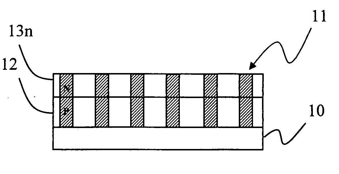
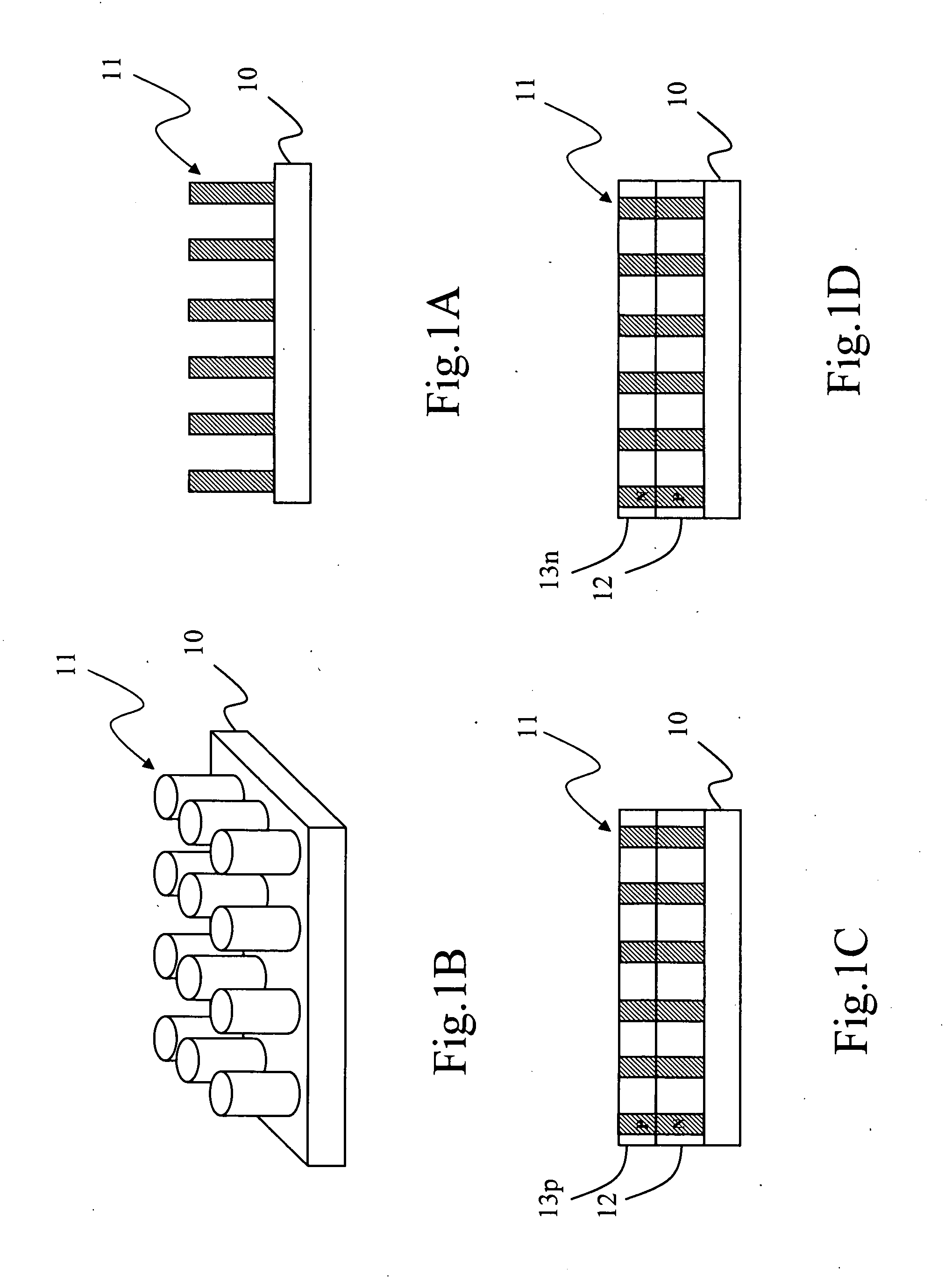
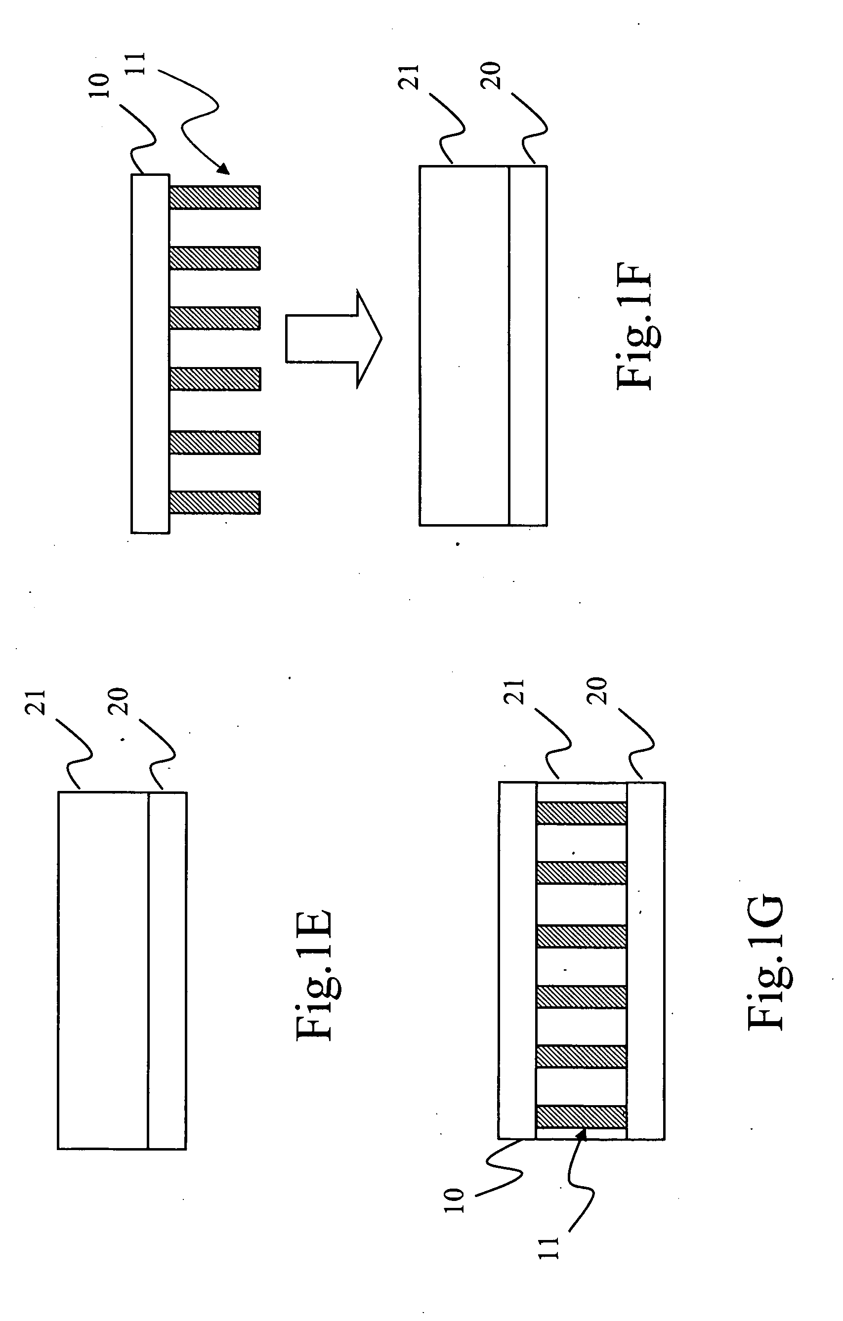
[0022]Refer to from FIG. 1A to FIG. 1H diagrams schematically showing a method for transferring a semiconductor micro / nanostructure array according to one embodiment of the present invention.

[0023]As shown in FIG. 1A and FIG. 1B, a source-material wafer 10 having a semiconductor micro / nanostructure array 11 is provided firstly. The semiconductor micro / nanostructure array 11 is made of an arbitrary semiconductor, such as an elemental semiconductor, a binary compound semiconductor, or a multi-component compound semiconductor (e.g. silicon, germanium, gallium arsenide, indium phosphide, gallium phosphide, antimony selenide, etc.). The longitudinal section of the semiconductor micro / nanostructure array 11 has a width of from 1 nm to 3000 μm and a length of from 50 nm to 50 μm. The length and width of the micro / nanostructure array 11 may vary with the absorption coefficient of the material. The source-material wafer 10 is made of an elemental semiconductor, a binary compound semiconducto...


PUM


Abstract

The present invention discloses a micro/nanostructure PN junction diode array thin-film solar cell and a method for fabricating the same, wherein a microstructure or sub-microstructure PN junction diode array, such as a nanowire array or a nanocolumns array, is transferred from a source-material wafer to two pieces of transparent substrates, which are respectively corresponding to two electric conduction types, to fabricate a thin-film solar cell. In the present invention, the micro/nanostructure PN junction diode array has advantages of a fine-quality crystalline semiconductor, and the semiconductor substrate can be reused to save a lot of semiconductor material. Besides, the present invention can make the best of sunlight energy via stacking up the solar cells made of different types of semiconductor materials to absorb different wavebands of the sunlight spectrum.

Description

BACKGROUND OF THE INVENTION[0001]1. Field of the Invention[0002]The present invention relates to a thin-film solar cell, particularly to a micro / nanostructure PN junction diode array thin-film solar cell and a method for fabricating the same.[0003]2. Description of the Related Art[0004]Petroleum is going to be exhausted by the end of this century, and the voice for substitute energies has been cried for a long time. Substitute energies include wind power, wave power, and biofuel. Among them, solar energy has relative higher market acceptability, and many nations have been devoted to the development of solar energy. The German Advisory Council on Global Change predicted that solar energy will provide about 60% of the total energy in 2100. Solar energy is generated by the photovoltaic effect, wherein solar energy material directly converts sunlight into electric energy. The crystalline silicon solar cell has been developed for tens of years, and the related technologies thereof have b...

Claims


Application Information

Patent Timeline
IPC IPC(8): H01L31/00H01L21/02H01L31/18
CPCB82Y10/00H01L27/301H01L29/6609H01L29/861H01L31/03529Y02E10/547H01L31/0392H01L31/068H01L31/1892H01L51/424Y02E10/549H01L31/0384H01L31/03926H10K39/10H10K30/20
Inventor LIN, CHING-FUHCHAO, JIUN-JIESHIU, SHU-CHIA
Owner NAT TAIWAN UNIV
Why Eureka
Try Eureka