Check patentability & draft patents in minutes with Patsnap Eureka AI!

Semiconductor device comprising capacitive element

Active Publication Date: 2010-12-30
RENESAS ELECTRONICS CORP
View PDF5 Cites 10 Cited by
  • Summary
  • Abstract
  • Description
  • Claims
  • Application Information

AI Technical Summary

Benefits of technology

[0013]In Patent Literature 1, the lower electrode and capacitive insulating film are successively formed so as to prevent oxygen defects. However, oxydation gas is used in a high temperature chamber for forming a film by ALD. Therefore, an unexpected oxide film is formed on the lower electrode surface, causing oxygen defects. Furthermore, a single film of metal oxide (particularly transition metal oxide) is subject to process (reduction) damage during formation of an upper electrode film or during etching, causing new oxygen defects in an insulating film. Then, leakage paths are increased and current leakage is significantly increased.
[0015]In Patent Literature 3, the silicon / metal composition ratio is adjusted to prevent the relative dielectric constant from being lowered by silicate. However, the silicon composition ratio should be increased both at the upper interface and at the lower interface of the film in order to realize low current leakage properties. The entire film is silicated and the relative dielectric constant is significantly lowered compared with a single film of metal oxide.
[0019]The semiconductor device of the present invention has a capacitive element undergoing little reduction in dielectric constant or little current leakage between the upper and lower electrodes, improving the efficiency of the semiconductor device.
[0020]The semiconductor device production method of the present invention can easily form a transition metal silicate film in which the silicon composition ratio is lowered stepwise towards the bottom and produces an insulating film preferably used particularly in a capacitive element for which low current leakage is desired.

Problems solved by technology

Therefore, an unexpected oxide film is formed on the lower electrode surface, causing oxygen defects.
Furthermore, a single film of metal oxide (particularly transition metal oxide) is subject to process (reduction) damage during formation of an upper electrode film or during etching, causing new oxygen defects in an insulating film.
Then, leakage paths are increased and current leakage is significantly increased.
Composed of only metal oxides, poor reduction damage resistance is observed.
Furthermore, oxygen defects occurring in the electrode / insulating film interface is not taken care of.
Therefore, oxygen defects occur in the insulating film and current leakage is significantly increased as in Patent Literature 1.

Method used


Image

  • Semiconductor device comprising capacitive element
  • Semiconductor device comprising capacitive element
  • Semiconductor device comprising capacitive element

Examples


embodiment 1

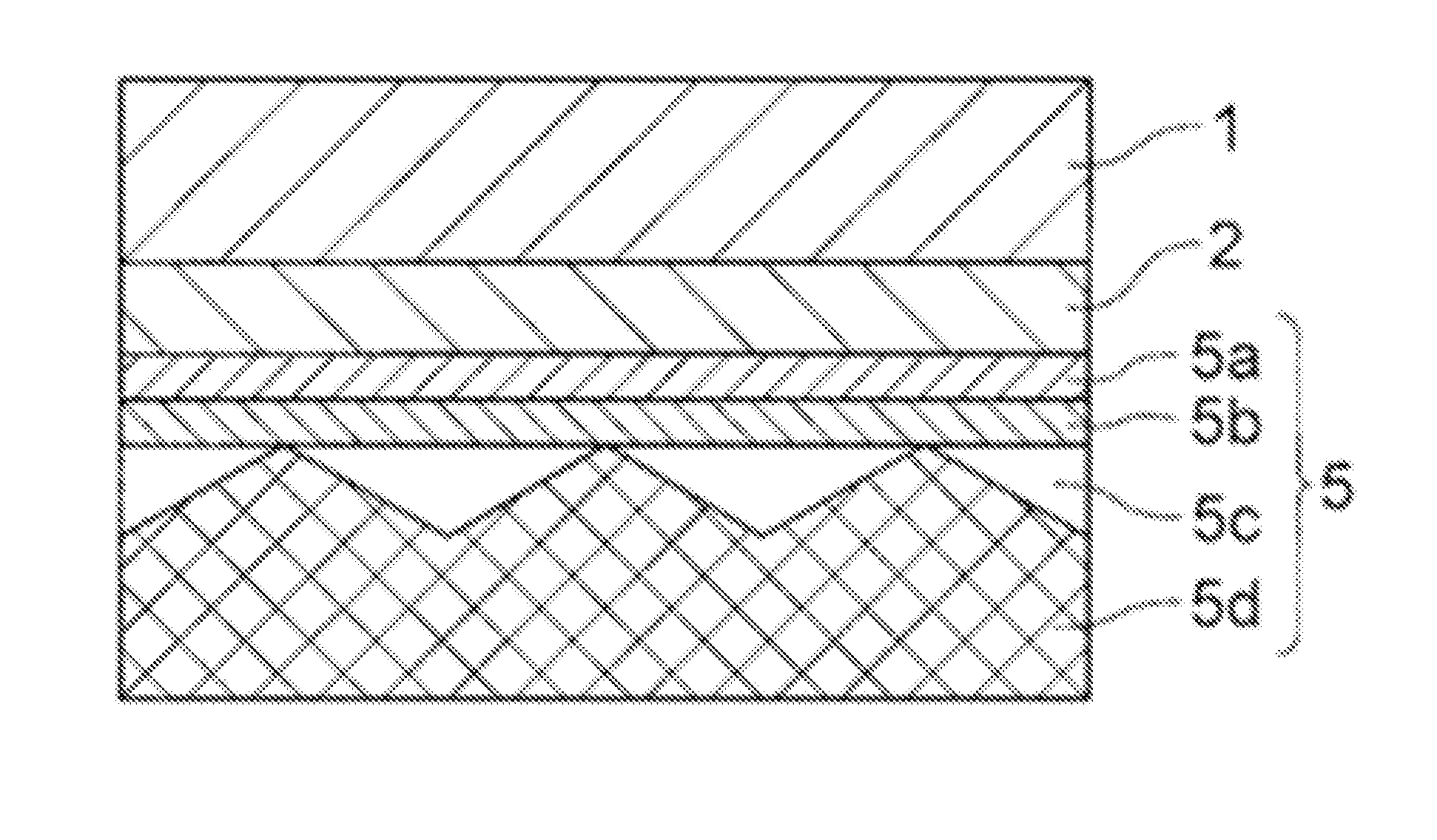
[0040]FIG. 1 is a cross-sectional view of the capacitive element in the semiconductor device according to Embodiment 1 of the present invention. The capacitive element includes an upper electrode film 1, a capacitive insulating film 2, and a lower electrode film 5. The lower electrode 5 is composed of a laminated film consisting of, for example, a thin titanium nitride film 5a, a tantalum nitride film 5b, a tantalum film 5c, and a titanium nitride film 5d. The capacitive insulating film 2 laminated on the lower electrode is composed of a tantalum oxide film or tantalum silicate film formed by plasma oxidation. Other examples of the plasma oxidized film include a film containing as the main constituent an oxide of any one or multiple metals among zirconium, hafnium, niobium, titanium, tungsten, cobalt, molybdenum, vanadium, lanthanum, manganese, chrome, yttrium, and praseodymium.

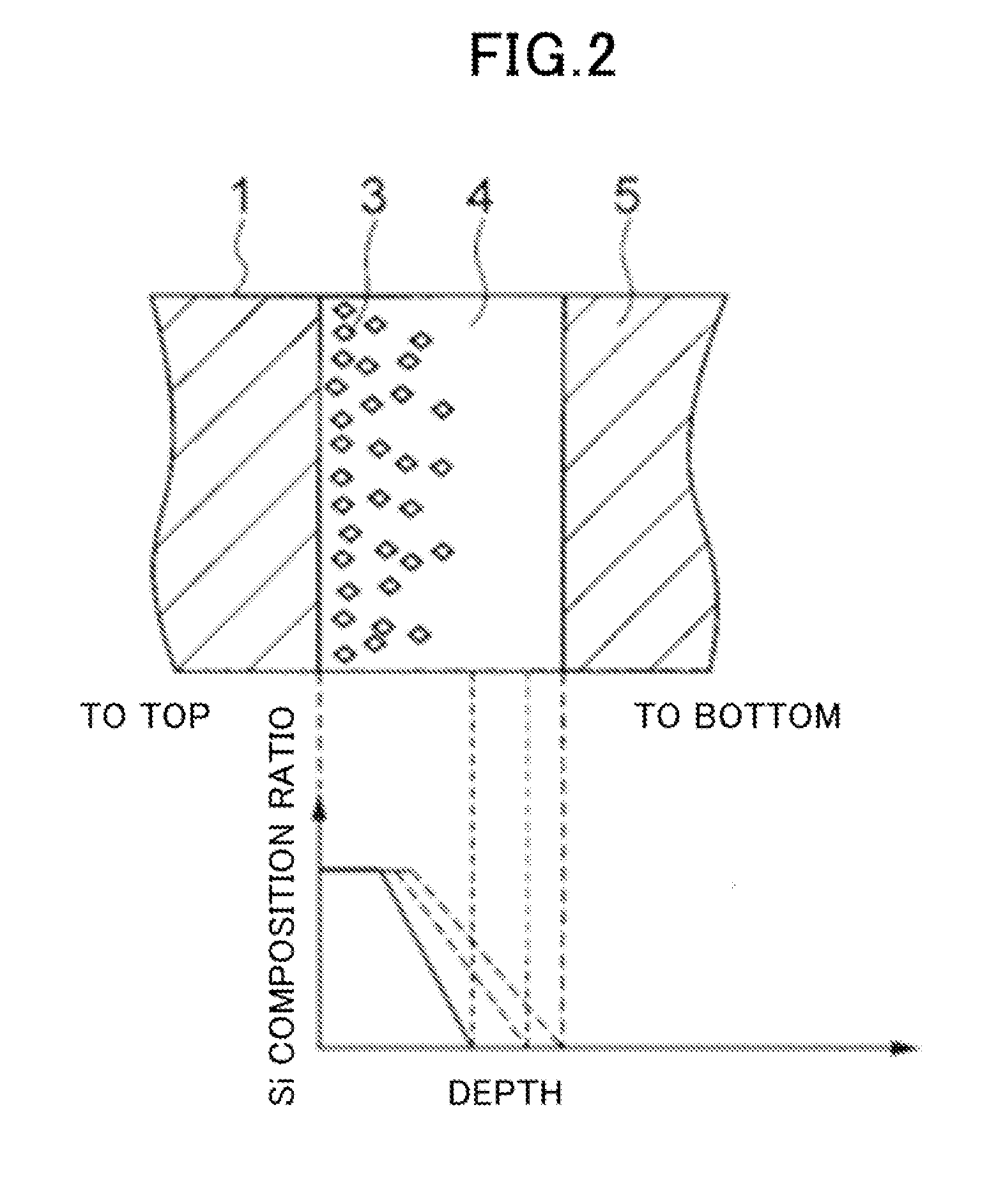
[0041]FIG. 2 shows the Si composition profile in the capacitive insulating film of Embodiment 1. In this f...

embodiment 2

[0056]The capacitive element of the semiconductor device of Embodiment 2 has an MIM structure installed in an actual ULSI wiring structure as shown in FIG. 10 (10-a to 10-o).

[0057]In a production process, first, a silicon oxide film 102 of 400 nm in thickness is formed on an underlying wire 101 by plasma CVD. Then, a polycrystalline titanium nitride film 103a of 100 nm in thickness, a microcrystalline tantalum film 103b of 30 nm in thickness, and a polycrystalline titanium nitride film 103c of 15 nm in thickness are sequentially formed as a lower electrode. A tantalum film 104 of 3 to 10 nm in thickness is formed thereon as a transition metal film. Then the tantalum film 104 is plasma-oxidized to form a tantalum oxide film, namely a capacitive insulating film 105. Here, the tantalum film 104 is desirably β-tantalum or an α-β mixed crystal system film containing a relatively large amount of β-tantalum. No inconvenience occurs even if the lower electrode has a two-layer structure comp...

embodiment 3

[0063]The capacitive element of the semiconductor device according to Embodiment 2 has an MIM structure installed in an actual ULSI wire structure as shown in FIG. 11 (11-a to 11-o).

[0064]In a production process, first, a silicon oxide film 202 of 400 nm in thickness is formed on a lower wire 201 by plasma CVD. A polycrystalline titanium nitride film 203 of 140 nm in thickness as a lower electrode and a tantalum film 204 of 3 to 10 nm in thickness as a transition metal film are formed. Then, the tantalum film 204 is irradiated with mono-silane gas to add silicon to it and then plasma-oxidized to form a tantalum silicate film 205. Here, the tantalum film 204 is desirably a β-tantalum or an α-β mixed crystal system film containing a large amount of β-tantalum. A titanium nitride film 206 of 100 nm in thickness as an upper electrode film and a silicon nitride film 207 of 250 nm in thickness as an upper electrode etching stopper are formed (FIG. 11-a). The lower electrode 203 can be a C...


PUM


Abstract

A capacitive element formed within a semiconductor device comprises an upper electrode, a capacitive insulating film containing an oxide and / or silicate of a transition metal element, and a lower electrode having a polycrystalline conductive film composed of a material having higher oxidation resistance than the transition metal element and an amorphous or microcrystalline conductive film formed below the polycrystalline conductive film.

Description

TECHNICAL FIELD[0001]The present invention relates to a semiconductor device comprising a capacitive element on a multilayer wiring structure or in a multilayer wiring and a production method thereof.BACKGROUND ART[0002]Conventional capacitive elements for high frequency devices or for decoupling are capacitive elements having a PIP (polysilicon / insulating film / polysilicon) structure in which polysilicon is used for both, upper and lower, electrodes or a MOS (polysilicon electrode / gate silicon oxide film / silicon substrate) structure. However, polysilicon electrodes have problems such as large resistance and depletion. MIM (metal / capacitive insulating film / metal) structures are employed in which a metal or metal oxide film, such as titanium nitride and ruthenium oxide, is used for the electrodes. To date, titanium oxide films are extensively studied for the electrodes in MIM structures. This is because the electrodes in an MIM structure have low electric resistance and easy to form b...

Claims


Application Information

Patent Timeline
IPC IPC(8): H01L29/92H01L21/314
CPCH01L21/31637H01L23/5223H01L23/5283H01L23/5286H01L27/0688H01L28/75H01L21/28506H01L2924/0002H01L21/32053H01L21/32105H01L28/60H01L2924/00H01L21/0215H01L21/02252H01L21/02244
Inventor KUME, IPPEIINOUE, NAOYAHAYASHI, YOSHIHIRO
Owner RENESAS ELECTRONICS CORP
Features
  • R&D
  • Intellectual Property
  • Life Sciences
  • Materials
  • Tech Scout
  • Unparalleled Data Quality
  • Higher Quality Content
  • 60% Fewer Hallucinations
Learn More