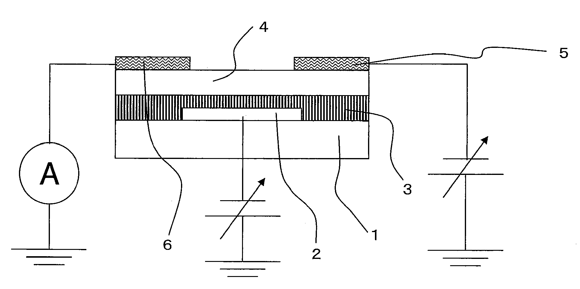
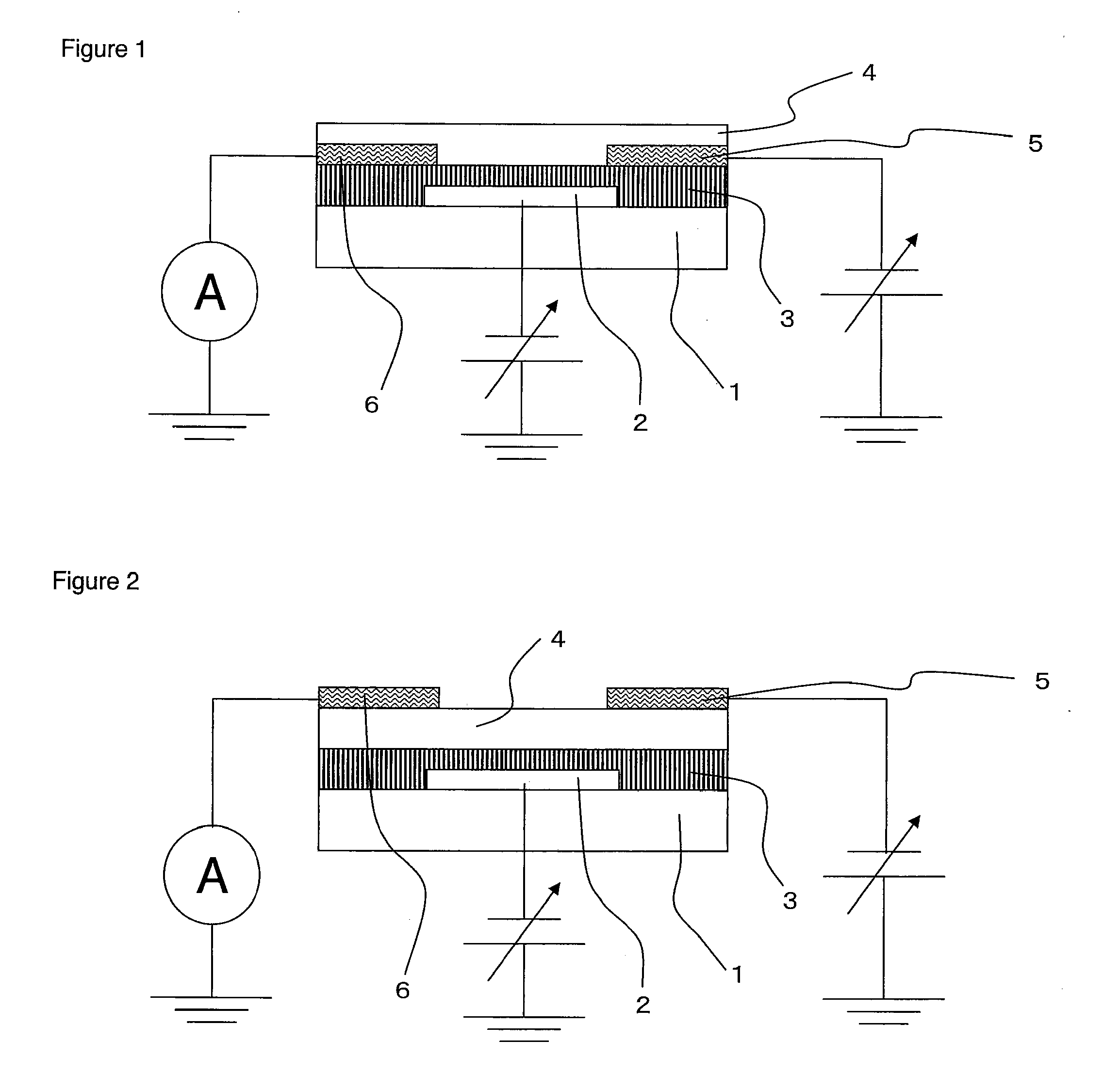
Gate insulating material, gate insulating film and organic field-effect transistor

a gate insulating film and organic field-effect technology, applied in the field of gate insulating film and organic field-effect transistor, can solve the problems of high temperature process, inorganic film formation is difficult, and inorganic film coating is not easy to achieve, and the effect of superior chemical resistance and coatability of resists

Inactive Publication Date: 2011-03-24
TORAY IND INC
View PDF1 Cites 15 Cited by
  • Summary
  • Abstract
  • Description
  • Claims
  • Application Information

AI Technical Summary

Benefits of technology

[0011]In accordance with the present invention, it is possible to provide a gate insulating material which is superior in chemical resistance and coatability of a resist and an organic semiconductor coating liquid, and realizes small hysteresis, a gate insulating film and an organic field-effect transistor using the same.

Problems solved by technology

Common gate insulating films include inorganic films of silicon oxide and the like, but since expensive vacuum equipment such as CVD equipment is required in order to form inorganic films, the cost is increased.
Further, this method has a problem that a high-temperature process is required for forming inorganic films and fabrication on a flexible substrate of plastic or the like is difficult.
However, since large amounts of polar groups such as an amino group and a phenol group remain in the materials, there is a problem of FET characteristics, particularly large hysteresis.
Further, if the gate insulating material has such polar groups, in the case of patterning by a resist, the polar group can cause the permeation of chemicals into the insulating film or swelling in the steps of application, development and stripping of the resist to degrade the insulating film.
Examples of other gate insulating films include a polysiloxane (for example, refer to Patent Documents 1 to 3), but a polysiloxane has a problem that, because of its high water repellency, the cissing of a coating liquid takes place in a process of applying a resist or an organic semiconductor onto a polysiloxane film and the formation of a uniform film is difficult.

Method used


Image

  • Gate insulating material, gate insulating film and organic field-effect transistor
  • Gate insulating material, gate insulating film and organic field-effect transistor
  • Gate insulating material, gate insulating film and organic field-effect transistor

Examples


example 1

(1) Preparation of Organic Semiconductor Composite Solution

[0117]0.10 g of poly(3-hexyl thiophene) (manufactured by Aldrich, regioregular, number average molecular weight (Mn): 13000, hereinafter referred to as P3HT) as a conjugated polymer was added to 5 ml of chloroform in a flask and the resulting mixture was mixed by ultrasonic agitation in an ultrasonic cleaner (US-2 manufactured by Iuchi Seieido Co., Ltd., output 120 W) to obtain a chloroform solution of P3HT. Next, this solution was taken with a dropper and added dropwise to a mixed solution of 20 ml of methanol and 10 ml of 0.1 N hydrochloric acid in 0.5 ml portions to perform reprecipitation. The solidified P3HT was collected through filtration by a membrane filter (manufactured by PTFE Co.: ethylene tetrafluoride) with a pore size of 0.1 μm and adequately rinsed with methanol, and then the solvent was eliminated by vacuum-drying. Dissolution and reprecipitation were repeated once more to obtain 90 mg of reprecipitated P3HT...

example 2

[0126]95.3 g (0.7 mol) of MTMSi, 24.6 g (0.1 mol) of β-EpETMSi and 39.7 g (0.2 mol) of PhTMSi were dissolved in 183 g of PGMB, and to the resulting solution, 55.8 g of water and 0.80 g of phosphoric acid were added while stirring the solution. The internal temperature of the resulting solution was raised to 90° C. by heating the solution in a bath of 105° C. for 2 hours to distill off components predominantly composed of methanol as a by-product. Next, the internal temperature of the solution was raised to 118° C. by heating the solution in a bath of 130° C. for 2 hours to distill off components predominantly composed of water and then the solution was cooled to room temperature to obtain a polysiloxane B having a solid concentration of 28.0% by weight. 50.0 g of the polysiloxane B obtained was weighed out and to this, 0.40 g of zirconia tetrakis(acetylacetonate) (hereinafter, referred to as ZrAcAc) as a zirconia-based curing agent was added, and the resulting mixture was mixed with...

example 3

[0127]40.9 g (0.3 mol) of MTMSi, 73.8 g (0.3 mol) of β-EpETMSi and 79.3 g (0.4 mol) of PhTMSi were dissolved in 231 g of propylene glycol monopropyl ether (boiling point 150° C., hereinafter, referred to as PGMP), and to the resulting solution, 59.4 g of water and 0.59 g of phosphoric acid were added while stirring the solution. The internal temperature of the resulting solution was raised to 90° C. by heating the solution in a bath of 105° C. for 2 hours to distill off components predominantly composed of methanol as a by-product. Next, the internal temperature of the solution was raised to 118° C. by heating the solution in a bath of 140° C. for 2 hours to distill off components predominantly composed of water and then the solution was cooled to room temperature to obtain a polysiloxane C having a solid concentration of 24.3% by weight. 50.0 g of the poly siloxane C obtained was weighed out and to this, 0.60 g of magnesium bis(acetylacetonate) (trade name NACEM magnesium, manufact...


PUM

PropertyMeasurementUnit
pressureaaaaaaaaaa
boiling pointaaaaaaaaaa
temperatureaaaaaaaaaa

Abstract

To provide a gate insulating material which has high chemical resistance, is superior in coatability of a resist and an organic semiconductor coating liquid, and has small hysteresis, a gate insulating film and an FET using the same by a polysiloxane having an epoxy group-containing silane compound as a copolymerization component.
A gate insulating material containing a polysiloxane having, as copolymerization components, at least a silane compound represented by the general formula (1):
R1mSi(OR2)4-m  (1),
    • wherein R1 represents hydrogen, an alkyl group, a cycloalkyl group, a heterocyclic group, an aryl group, a heteroaryl group or an alkenyl group and in the case where a plurality of R1s are present, R1s may be the same or different, R2 represents an alkyl group or a cycloalkyl group and in the case where a plurality of R2s are present, R2s may be the same or different, and m represents an integer of 1 to 3,
    • and an epoxy group-containing silane compound represented by the general formula (2):
R3nR4lSi(OR5)4-n-1  (2),
    • wherein R3 represents an alkyl group or a cycloalkyl group having one or more epoxy groups in a part of a chain and in the case where a plurality of R3s are present, R3s may be the same or different, R4 represents hydrogen, an alkyl group, a cycloalkyl group, a heterocyclic group, an aryl group, a heteroaryl group or an alkenyl group and in the case where a plurality of R4s are present, R4s may be the same or different, R5 represents an alkyl group or a cycloalkyl group and in the case where a plurality of R5s are present, R5s may be the same or different, l represents an integer of 0 to 2, and n represents 1 or 2 (however, l+n≦3).

Description

TECHNICAL FIELD[0001]The present invention relates to a gate insulating material, a gate insulating film and an organic field-effect transistor.BACKGROUND ART[0002]In recent years, there have been proposed organic field-effect transistors (hereinafter, referred to as an organic FET) using an organic semiconductor having excellent moldability as a semiconductor layer. Since a circuit pattern can be formed directly on a substrate through an ink-jet technique or screening technique by using the organic semiconductor as an ink, organic FETs using the organic semiconductor are actively studied in place of conventional field-effect transistors (hereinafter, referred to as an FET) using inorganic semiconductors. An important measure of FET performance is mobility. An improvement in the mobility means an increase in an ON-current. This means that a switching characteristic of the FET is improved, and for example, in liquid crystal display devices, this leads to realization of high gradation...

Claims


Application Information

Patent Timeline
Patent Type & Authority Applications(United States)
IPC IPC(8): H01L29/78
CPCC08G59/306H01B3/46C08G65/20C08G77/14C09D163/00H01L21/02126H01L21/02216H01L21/02282H01L21/3122H01L51/0036H01L51/0068H01L51/052H01L51/0545G03F7/0757H01B3/40C08G59/3281H10K85/113H10K85/655H10K10/471H10K10/466
Inventor MURASE, SEIICHIROFUJIWARA, TAKENORIJO, YUKARITSUKAMOTO, JUN
Owner TORAY IND INC
Why Eureka
Try Eureka