Method of Gallium Nitride growth over metallic substrate using Vapor Phase Epitaxy

a gallium nitride and epitaxy technology, applied in the direction of crystal growth process, polycrystalline material growth, transportation and packaging, etc., can solve the problem of limiting the practical use of these materials, the absence of native substrate, and the high defect densities of the obtained epitaxial films, so as to reduce the amount of absorbed impurities, the surface roughness is low, and the effect of avoiding scratches or steps

Inactive Publication Date: 2011-05-19
ZHU MINGWEI +2
View PDF2 Cites 7 Cited by
  • Summary
  • Abstract
  • Description
  • Claims
  • Application Information

AI Technical Summary

Benefits of technology

[0009]An objective of present invention is to provide a method for compound semiconductor, in particular AIN, GaN, InN and their compounds, crystal growth that makes use of the new class of substrates to improve the current technology in aspects of—including, but not limited to—cost reduction, thermal management, substrate removal and / or patterning, and crystal quality.
[0012]In another embodiment of the invention, no lattice match between the substrate and the deposited materials is used. Instead, the surface of the metallic substrate is prepared in such a way that it is nearly ideal crystalline surface, with low surface roughness, absence of scratches or steps, and with minimal contamination of absorbed impurities. By the use of the same technique as described above for the prevention of the substrate's reaction with the chemical components of the deposition, the high quality epitaxial layers of Nitrides are also obtained due to the absence of the defects in the substrate's morphology that would translate into the epitaxial layer's defects.
[0013]In yet another embodiment of the present invention, the growth is performed on the polycrystalline metal substrate of arbitrary shape, for example metal wire, while the high crystalline quality of the grown semiconductor is achieved due to the regrowth effect.

Problems solved by technology

Yet the most limiting factor for these materials' practical usage is the absence of the native substrate.
The use of other materials as a substrate results in high defect densities in the obtained epitaxial films due to crystalline lattice mismatch, differences in thermal expansion coefficients and nucleation imperfectness.
In addition, Sapphire substrate has much lower thermal conductivity than Gallium Nitride itself and therefore limits the power dissipation of the devices and structures formed on it; Silicon Carbide remains extremely expensive and therefore not suitable for consumer applications; and Silicon has the largest lattice mismatch and therefore highest arising defect density among these popular substrates.
At the same time, the Pulsed Laser Deposition technique has several important limitations, such as the necessity of switching the process chemicals' sources while fabricating the structure that consists of several layers of different Al, Ga and In composition; the inability of gradual change in composition, etc.

Method used


Image

  • Method of Gallium Nitride growth over metallic substrate using Vapor Phase Epitaxy
  • Method of Gallium Nitride growth over metallic substrate using Vapor Phase Epitaxy
  • Method of Gallium Nitride growth over metallic substrate using Vapor Phase Epitaxy

Examples


Embodiment Construction

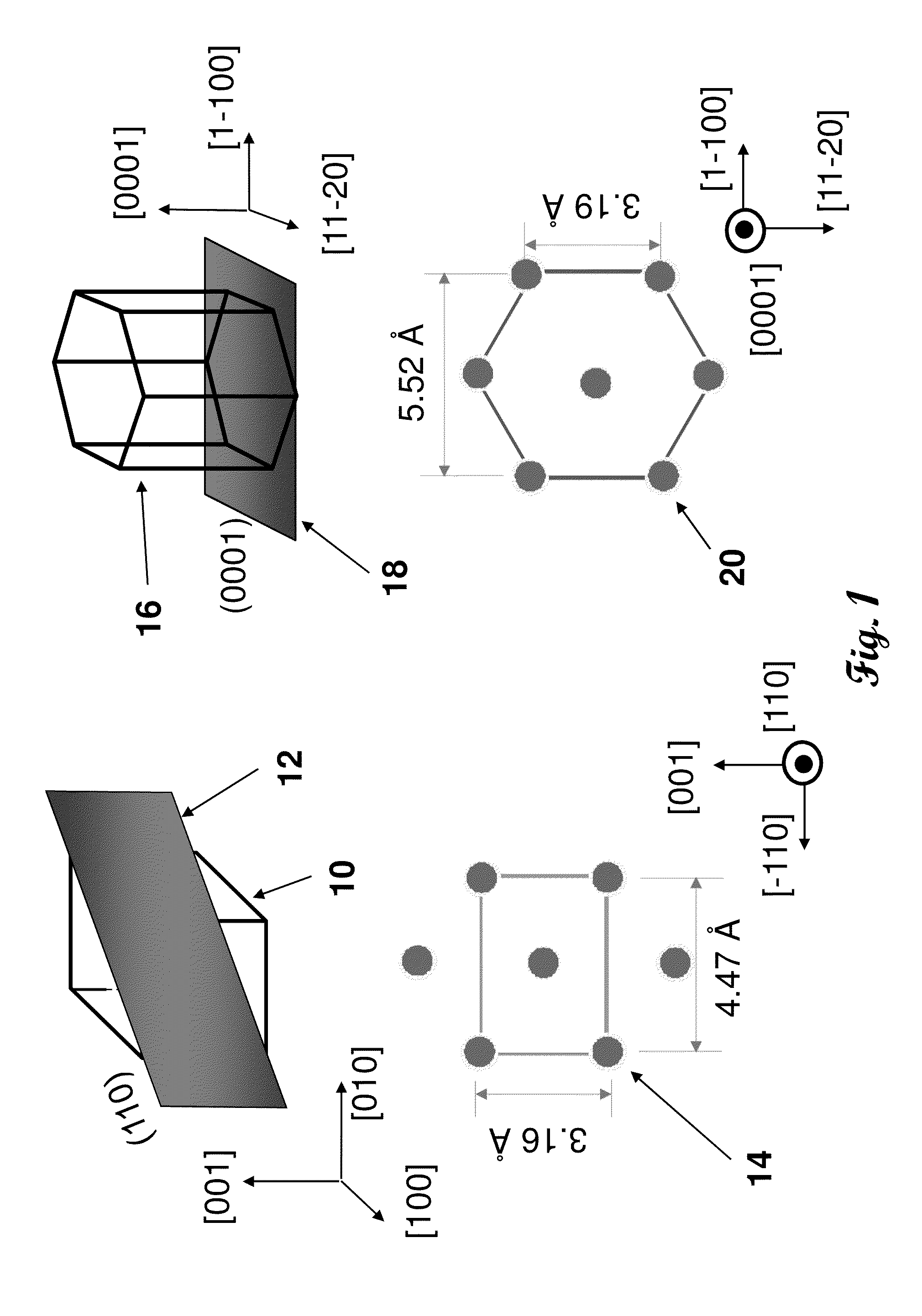
[0026]FIG. 1 depicts schematically the two-dimensional projection 10 of the three-dimensional elementary atomic cell of crystalline tungsten in alpha-phase and position of the (110) crystalline plane 12 crossing the said elementary cell. The atoms' arrangement 14 within the said (110) plane is provided, with the linear dimensions given in Angstroms. For comparison, the c-plane of wurtzite GaN (002) with atoms' arrangement 16 with the linear dimensions given in Angstroms is also presented. Along one of the axes, the atoms arrangement within the said planes represents nearly perfect lattice matching, with the mismatch value as low as 1%.

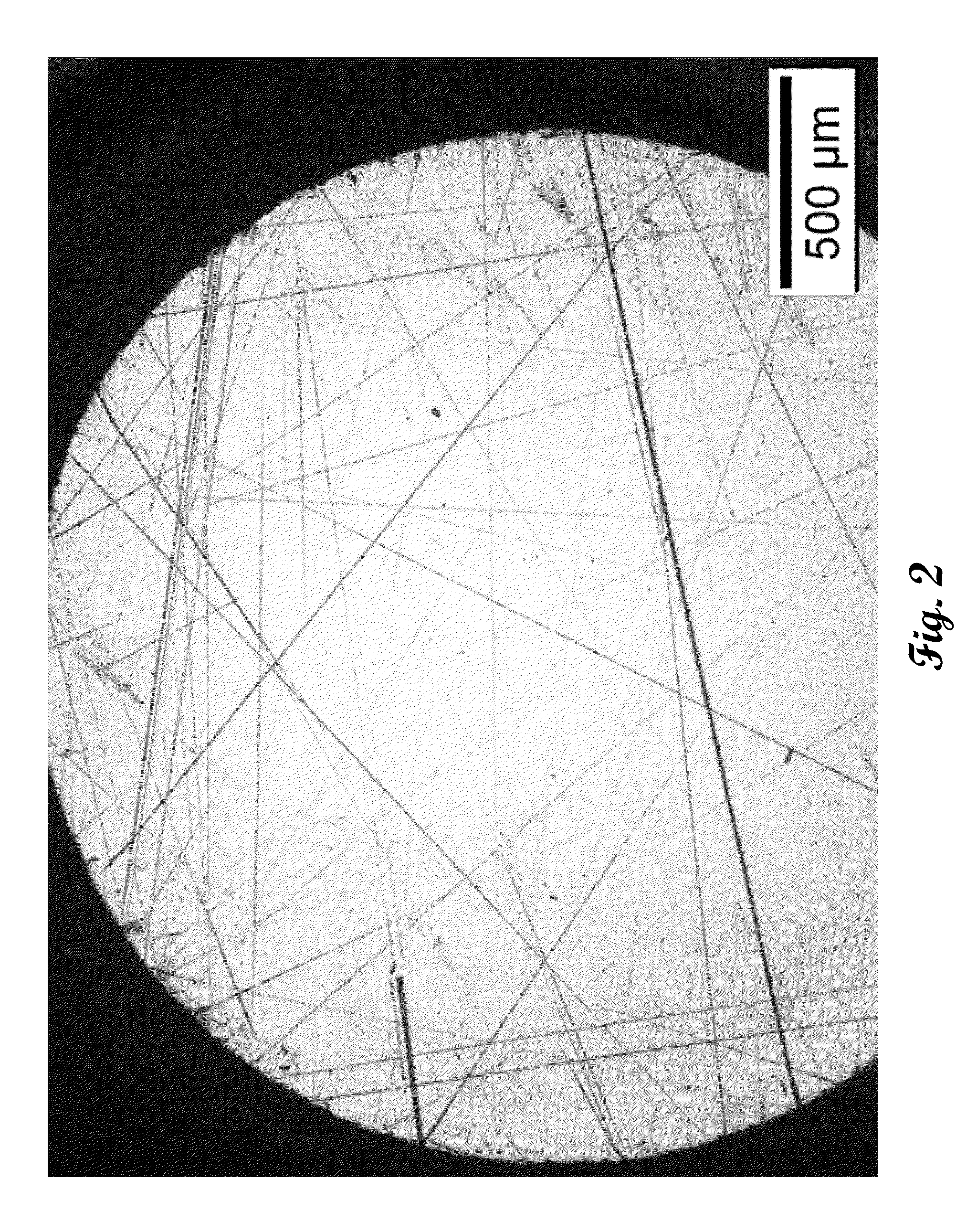
[0027]The example substrates for the present invention were prepared using the slicing of a single crystal tungsten rod. The diameter of the said rod was 3 mm. FIG. 2 presents the microphotograph of the surface of single crystal tungsten substrate prepared for MOVPE deposition. The scratches seen in the FIG. 2 resulted from mechanical polishing. It is ...


PUM

PropertyMeasurementUnit
temperatureaaaaaaaaaa
melting pointaaaaaaaaaa
diameteraaaaaaaaaa

Abstract

The current invention introduces a method of crystal film's growth of Gallium Nitride and related alloys over a novel class of the substrates using Vapor Phase Epitaxy technique. This said novel class of the substrates comprises single crystal lattice matched, partially matched or mismatched metallic substrates. The use of such substrates provides exceptional thermal conductivity and application flexibility, since they can be easily removed or patterned by chemical etching for the purposes of additional contact formation, electromagnetic radiation extraction, packaging or other purposes suggested or discovered by the skilled artisan. In particular, if patterned, the remaining portions of the said substrates can be utilized as contacts to the semiconductor layers grown on them. In addition, the said metallic substrates are significantly more cost effective than most of the conventional substrates. The use of Vapor Phase Epitaxy allows growing the epitaxial layers with different and / or variable alloy composition, as well as heterostructures and superlattices.

Description

FIELD OF THE DISCLOSURE[0001]Aspects of the invention relate to the compound semiconductor material growth technique over the crystalline metallic substrate, and in particular, to the Vapor Phase Epitaxy (VPE) of Gallium Nitride, Indium Nitride, Aluminum Nitride and their combinative compounds over the crystalline Tungsten substrate.BACKGROUND OF THE DISCLOSURE[0002]Gallium Nitride and related alloys (Indium Nitride, Aluminum Nitride and their ternary and quaternary alloys) are known for their potential applications in semiconductor industry, in particular in electronics and optoelectronics. Yet the most limiting factor for these materials' practical usage is the absence of the native substrate. Instead, the single crystal Sapphire, Silicon Carbide or Silicon substrates are commonly used to grow epitaxial films of Gallium Nitride and related alloys.[0003]The use of other materials as a substrate results in high defect densities in the obtained epitaxial films due to crystalline latt...

Claims


Application Information

Patent Timeline
Patent Type & Authority Applications(United States)
IPC IPC(8): C30B25/18B32B15/04
CPCC30B29/403C30B25/183Y10T428/31678
Inventor ZHU, MINGWEIDETCHPROHM, THEERADETCHWETZEL, CHRISTIAN
Owner ZHU MINGWEI
Why Eureka
Try Eureka