Thin film transistor and display
a thin film transistor and display technology, applied in the field of thin film transistors, can solve the problems of difficult to form tfts, low heat stability of pentacene, and inability to realize practical devices, and achieve the effects of low cost, small subthreshold swing value, and high on/off current ratio
- Summary
- Abstract
- Description
- Claims
- Application Information
AI Technical Summary
Benefits of technology
Problems solved by technology
Method used
Image

Examples
first embodiment
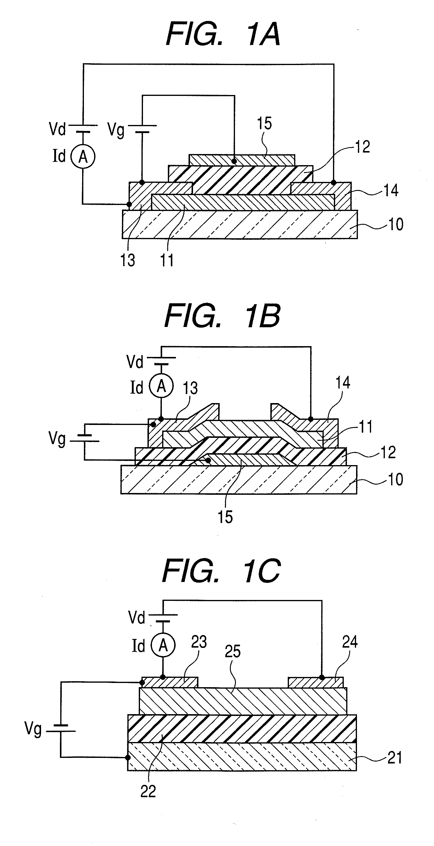
[0253]FIG. 1A illustrates a schematic sectional view of a top gate field effect transistor that has an amorphous In—Ge—O channel layer according to this embodiment.
[0254]As illustrated in FIG. 1A, an amorphous In—Ge—O oxide film is formed as a channel layer on a glass substrate (Corning 1737, manufactured by Corning Incorporated). The In—Ge—O amorphous oxide film is formed by a high frequency sputtering method in a mixed-gas atmosphere of argon and oxygen inside a sputtering chamber.
[0255]FIG. 13 is a diagram outlining a film deposition system that is used to form a film as a channel layer of a field effect transistor according to an embodiment of the present invention.
[0256]As illustrated in FIG. 13, the film formation system of this embodiment has a gate valve 57 for controlling the vacuum pumping ability and a mass flow controller 56 provided for each gas system in order to control the amount of gas flowing into the gas system. The film formation system also has a vacuum ion gaug...
second embodiment
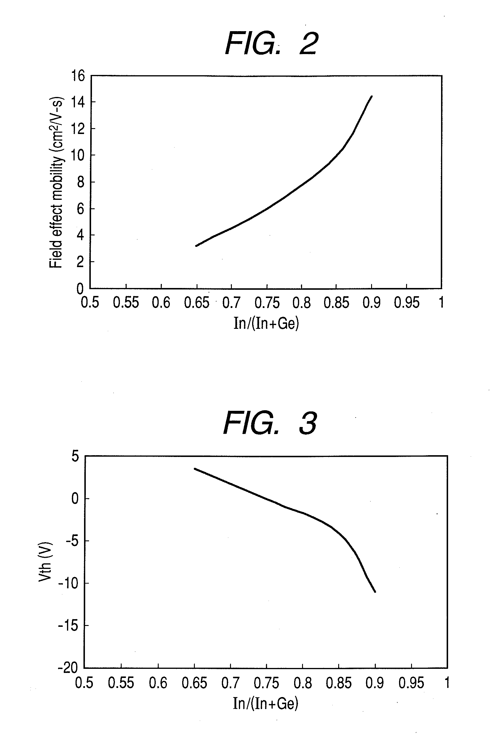
[0289]This embodiment is an example of studying the material composition dependency of a channel layer.
[0290]In order to examine the material composition dependency, a combinatorial method is employed for deposition. Specifically, the examination has been made with the use of a method in which an oxide thin film varied in composition is formed on a single substrate at once by a sputtering method.
[0291]However, this method does not always need to be employed. Material sources (targets) of a given composition may be prepared for deposition, or a thin film of desired compositions may be formed by controlling the input power applied to each of multiple targets.
[0292]An oxide thin film in which a composition distribution is observed has been formed on a substrate by a combinatorial sputtering method. Through a device fabrication process, TFTs that have various channel compositions were fabricated on the substrate at once. The TFTs were subsequently evaluated and compared.
[0293]An In—Ge—O...
third embodiment
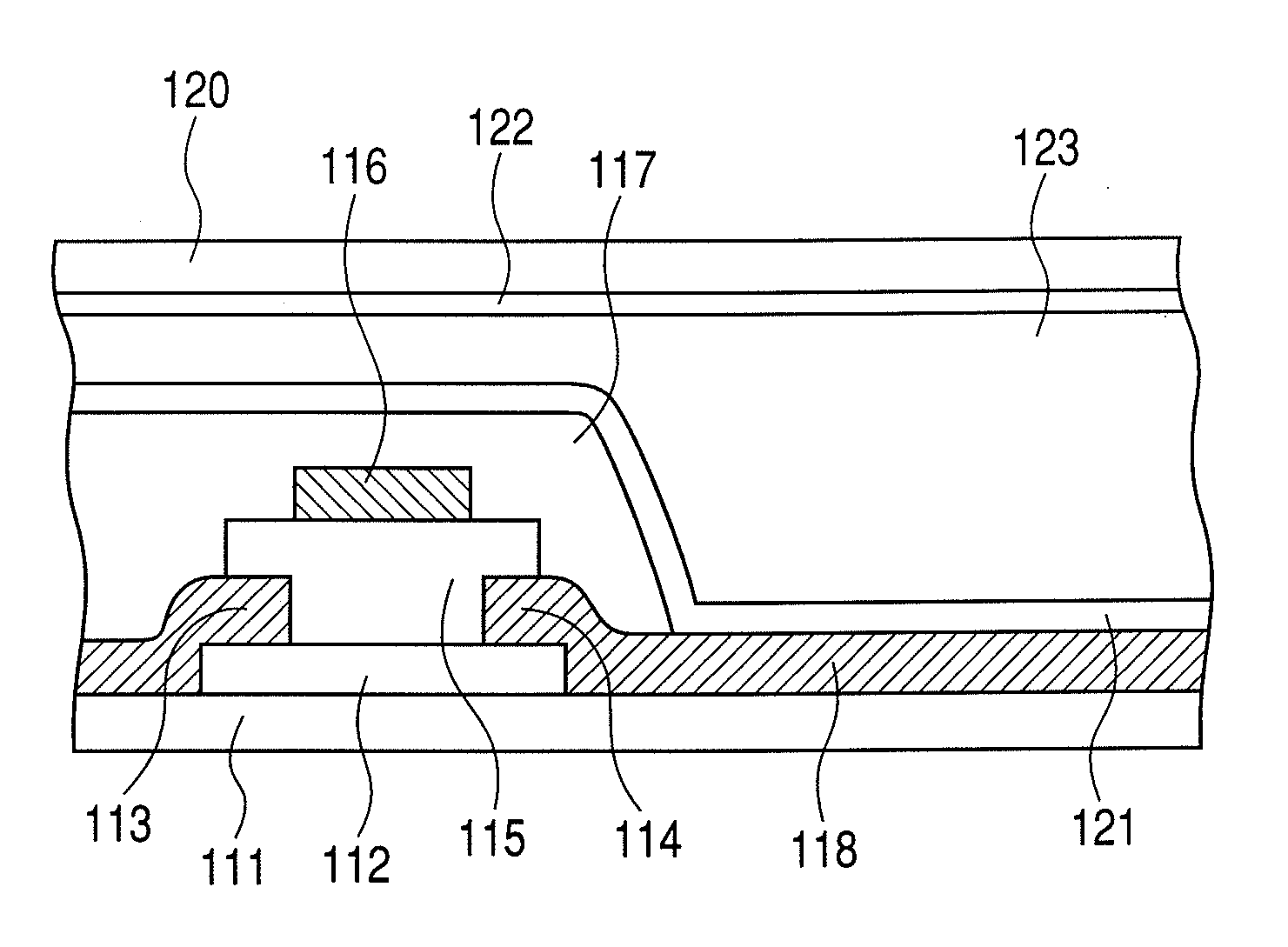
[0382]This embodiment is an example of using an amorphous In—Ge—O oxide semiconductor as a channel layer on a plastic substrate.
[0383]A structural example of a thin film transistor of this embodiment is illustrated in FIG. 1B. The length of the channel is 60 μm, and the width of the channel is 180 μm. The substrate 10 is a polyethylene terephthalate (PET) film.
[0384]First, the gate electrode 15 and the gate insulation layer 12 are formed by patterning on the substrate 10 with the use of the photolithography patterning method and the lift-off method.
[0385]The gate electrode 15 is a Ta layer having a thickness of 50 nm. The gate insulation layer is an SiOxNy film formed by sputtering to a thickness of 150 nm. The dielectric constant of the SiOxNy film is about 6.
[0386]Next, the channel layer of the transistor was formed by sputtering and shaped by photolithography patterning and lift-off.
[0387]The channel layer 11 is made of an In—Zn—Ge—O-based amorphous oxide and has a composition ex...
PUM
| Property | Measurement | Unit |
|---|---|---|
| specific resistivity | aaaaa | aaaaa |
| off-current | aaaaa | aaaaa |
| DC drive stress | aaaaa | aaaaa |
Abstract
Description
Claims
Application Information
 - R&D
- Intellectual Property
- Life Sciences
- Materials
- Tech Scout
- Unparalleled Data Quality
- Higher Quality Content
- 60% Fewer Hallucinations
Browse by: Latest US Patents, China's latest patents, Technical Efficacy Thesaurus, Application Domain, Technology Topic, Popular Technical Reports.
© 2025 PatSnap. All rights reserved.Legal|Privacy policy|Modern Slavery Act Transparency Statement|Sitemap|About US| Contact US: help@patsnap.com