Eureka AIR delivers breakthrough ideas for toughest innovation challenges, trusted by R&D personnel around the world.

Antireflective coating composition and process thereof

Inactive Publication Date: 2012-10-04
AZ ELECTRONICS MATERIALS USA CORP
View PDF0 Cites 14 Cited by
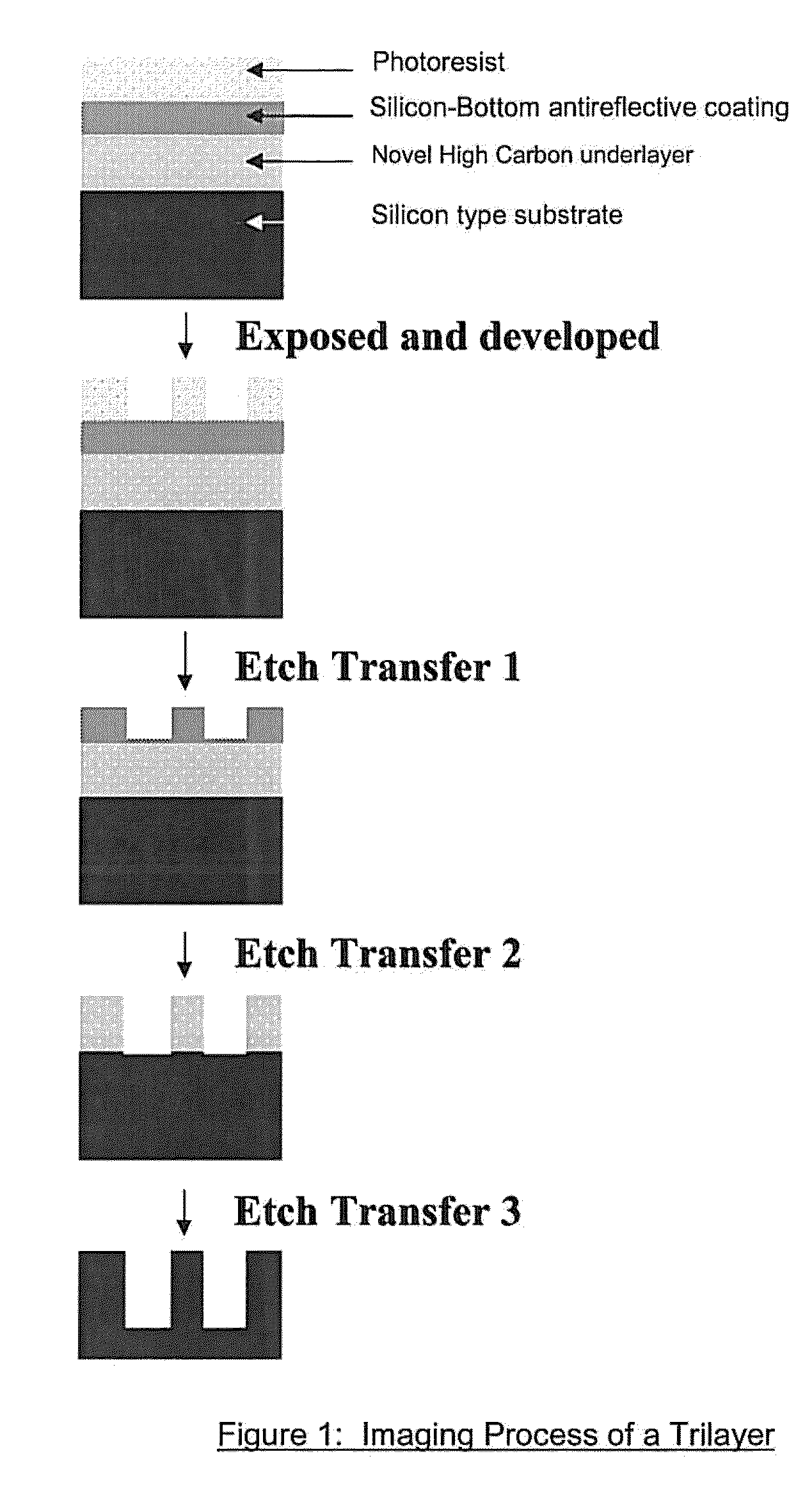
  • Summary
  • Abstract
  • Description
  • Claims
  • Application Information

AI Technical Summary

Benefits of technology

[0005]Absorbing antireflective coatings and underlayers in photolithography are used to diminish problems that result from back reflection of light from highly reflective substrates. Two major disadvantages of back reflectivity are thin film interference effects and reflective notching. Thin film interference, or standing waves, result in changes in critical line width dimensions caused by variations in the total light intensity in the photoresist film as the thickness of the photoresist changes or interference of reflected and incident exposure radiation can cause standing wave effects that distort the uniformity of the radiation through the thickness. Reflective notching becomes severe as the photoresist is patterned over reflective substrates containing topographical features, which scatter light through the photoresist film, leading to line width variations, and in the extreme case, forming regions with complete photoresist loss. An antireflective coating coated beneath a photoresist and above a reflective substrate provides significant improvement in lithographic performance of the photoresist. Typically, the bottom antireflective coating is applied on the substrate and then a layer of photoresist is applied on top of the antireflective coating. The antireflective coating is cured to prevent intermixing between the antireflective coating and the photoresist. The photoresist is exposed imagewise and developed. The antireflective coating in the exposed area is then typically dry etched using various etching gates, and the photoresist pattern is thus transferred to the substrate. Multiple antireflective layers and underlayers are being used in new lithographic techniques. In cases where the photoresist does not provide sufficient dry etch resistance, underlayers or antireflective coatings for the photoresist that act as a hard mask and are highly etch resistant during substrate etching are preferred, and one approach has been to incorporate silicon into a layer beneath the organic photoresist layer. Additionally, another high carbon content antireflective or mask layer is added beneath the silicon antireflective layer, which is used to improve the lithographic performance of the imaging process. The silicon layer may be spin coatable or deposited by chemical vapor deposition. Silicon is highly etch resistant in processes where O2 etching is used, and by providing a organic mask layer with high carbon content beneath the silicon antireflective layer, a very large aspect ratio can be obtained. Thus, the organic high carbon mask layer can be much thicker than the photoresist or silicon layer above it. The organic mask layer can be used as a thicker film and can provide better substrate etch masking that the original photoresist.
[0006]The present invention relates to a novel organic spin coatable antireflective coating composition or organic mask underlayer which has high carbon content, and can be used between a photoresist layer and the substrate as a single layer of one of multiple layers. Typically, the novel composition can be used to form a layer beneath an essentially etch resistant antireflective coating layer, such as a silicon antireflective coating. The high carbon content in the novel antireflective coating, also known as a carbon hard mask underlayer, allows for a high resolution image transfer with high aspect ratio. The novel composition is useful for imaging photoresists, and also for etching the substrate. The novel composition enables a good image transfer from the photoresist to the substrate, and also reduces reflections and enhances pattern transfer. Additionally, substantially no intermixing is present between the antireflective coating and the film coated above it. The antireflective coating also has good solution stability and forms films with good coating quality, the latter being, particularly advantageous for lithography.SUMMARY OF THE INVENTION

Problems solved by technology

Two major disadvantages of back reflectivity are thin film interference effects and reflective notching.
Thin film interference, or standing waves, result in changes in critical line width dimensions caused by variations in the total light intensity in the photoresist film as the thickness of the photoresist changes or interference of reflected and incident exposure radiation can cause standing wave effects that distort the uniformity of the radiation through the thickness.

Method used


Image

  • Antireflective coating composition and process thereof
  • Antireflective coating composition and process thereof
  • Antireflective coating composition and process thereof

Examples


example 1

Synthesis of copolymer of 2-phenylphenol / divinylbenzene / a-anthracenemethanol

[0047]A solution was prepared consisting of 12.76 g (0.075 mol) 2-phenylphenol, 15.62 g (0.075 mol) 9-Anthracene Methanol, 9.76 (0.075 mol) divinylbenzene dissolved in 25 g cyclopepentyl methyl ether (CPME) and 90 g diethylelene glycol dimethyl ether (DEGME) and the mixture was stirred for 5 minutes in a 250 mL, 4 neck flask equipped with an overhead mechanical stirrer, condenser, thermo watch, Dean Stark trap and an N2 purge. After this time, 1.14 g of triflic acid (3% wt of monomers) was added to the stirred mixture and it was stirred for another 5 minutes. The temperature of the stirred mixture was then raised to 140° C. and heated for 3 hours. After cooling the reaction mixture and diluting it with 250 mL of CPME, it was transferred to a separatory funnel, and it was washed with two aliquots of deionised (DI) water (2×200 mL). The polymer was precipitated by drowning into hexane. The polymer was filtered...

example 2

Processing

[0048]The polymer of Example 1 was dissolved in PGMEA as a 7% wt solution. This solution was filtered through a 0.2μm PTFE filter and the solution was applied to silicon water and spun at 1,500 rpm to form a 200 micron thick polymer film. The coating quality of this polymer from a spin casting solvent was good with no visible defects present. Prior to post-applied bake (PAB), the coating passed an edgebead removal (EBR) test with PGMEA showing clean removal of polymer at the water's edge where the PGMEA solvent was applied. After PAB (230° or 400° C.), the coatings passed a soak tests with PGMEA solvent showing no visible sign of any film thickness loss. After PAB processing at different temperatures the polymer showed the following elemental composition.

230° bake400° bake% C89.6480.88% H5.923.72% O2.828.72

[0049]With a PAB of 250° C. this polymer coating gave n=1.47 and k=0.68

[0050]Six additional batches were made of this material including one which was scaled up tenfold....

example 3

Synthesis of co polymer of 2-phenylphenol / divinylbenzene / a-anthracenemethanol

[0051]Using the same setup as described for Example 1, 8.50 g (0.06 mol) 2-phenylphenol, 30.34 g (0.15 mol) 9-anthracene methanol, 13.0 g (0.10 mol) divinylbenzene, 45 g CPME and 160 g DEGME were used. As in Example 1, after stirring this solution for 5 minutes, 1.55 g (3% wt of monomers) triflic acid was added and the reaction was stirred for another 5 minutes. As in example 1, the reaction temperature was increased to 140° C. and heated for 5 hours. After cooling the reaction mixture and diluting it with 250 mL of CPME, it was transferred to a separatory funnel, and it was washed with two aliquots of DI water (2×200 mL). The polymer was then precipitated into hexane. The polymer was then washed with hexane, air dried by suction and finally dried in a vacuum oven overnight. This process yielded 45% finished polymer from the starting materials. The weight average molecular weight of the polymer was 1,727 wi...


PUM


Abstract

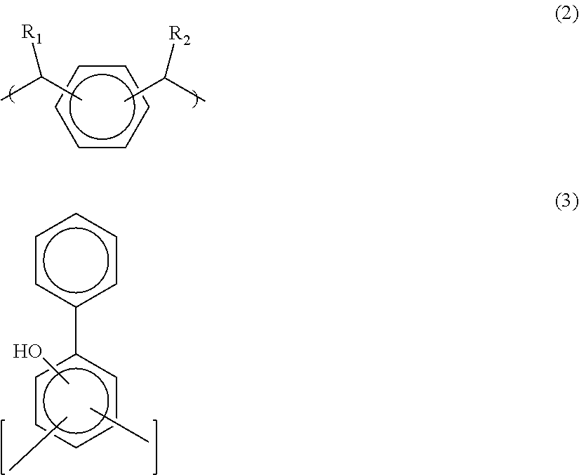
The invention relates to an antireflective coating composition comprising a crosslinker and a crosslinkable polymer capable of being crosslinked by the crosslinker, where the crosslinkable polymer comprises a unit represented by structure (1):A-B—C  (1)where A is a fused aromatic ring, B has a structure (2), and C is a hydroxybiphenyl of structure (3)where R1 is C1-C4alkyl and R2 is C1-C4alkyl.The invention further relates to a process for forming an image using the composition.

Description

[0001]The present invention relates to an absorbing hard mask antireflective coating composition comprising a polymer, where the polymer comprises in the backbone of the polymer at least one phenyl unit, at least one hydroxybiphenyl unit, and at least one substituted or unsubstituted fused aromatic ring, and a process for forming an image using the antireflective coating composition. The process is especially useful for imaging photoresists using radiation in the deep and extreme ultraviolet (uv) region.[0002]Photoresist compositions are used in microlithography processes for making miniaturized electronic components such as in the fabrication of computer chips and integrated circuits. Generally, in these processes, a thin coating of film of a photoresist composition is first applied to a substrate material, such as silicon based wafers used for making integrated circuits. The coated substrate is then baked to evaporate any solvent in the photoresist composition and to fix the coati...

Claims


Application Information

Patent Timeline
IPC IPC(8): G03F7/20G03F7/004C09K3/00
CPCG03F7/091
Inventor RAHMAN, M. DALILMCKENZIE, DOUGLASSHAN, JIANHUICHO, JOON YEONMULLEN, SALEM K.
Owner AZ ELECTRONICS MATERIALS USA CORP
Why Eureka
Eureka Blog
Learn More