Semiconductor-Graphene Hybrids Formed Using Solution Growth

a technology of semiconductors and graphene, which is applied in the direction of material nanotechnology, transportation and packaging, coatings, etc., can solve the problems of reducing the conductivity of graphene, reducing the reducing the band gap of graphene, so as to achieve high electrical conductivity of charge carriers, the effect of high mobility

Inactive Publication Date: 2013-04-25
UNIVERSITY OF KANSAS
View PDF3 Cites 64 Cited by
  • Summary
  • Abstract
  • Description
  • Claims
  • Application Information

AI Technical Summary

Benefits of technology

[0010]In another aspect, the growth methods of the present invention provide for a well formed interface between the graphene sheet and micro/nanostructures of the functional materials.
[0011]The development of such semiconductor-graphene hybrid micro/nanostructure systems using the solution growth methods of the present invention offer several advantages. Advantages of the hybrid system include, but are not limited to, high mobility and hence high electrical conductivity of charge carriers (due to graphene), extremely thin electrode (graphene may be one layer of carbon atoms), flexibility (if the graphene is supported by flexible support), low cost, and scalability to large scale. For example

Problems solved by technology

However, the zero bandgap of the graphene has presented a major hurdle to its electronic applications, especially in digital electronics.
(2009)), it is often at the cost of significantly reduced mobility due to the presence of charge fluctuation associated with various defects primarily from the uncontrolled GNR edges and the interfaces.
In addition, the high ZnO growth temperature may lead to forma

Method used


Image

  • Semiconductor-Graphene Hybrids Formed Using Solution Growth
  • Semiconductor-Graphene Hybrids Formed Using Solution Growth
  • Semiconductor-Graphene Hybrids Formed Using Solution Growth

Examples


example 1

Synthesis of ZnO Graphene Hybrids

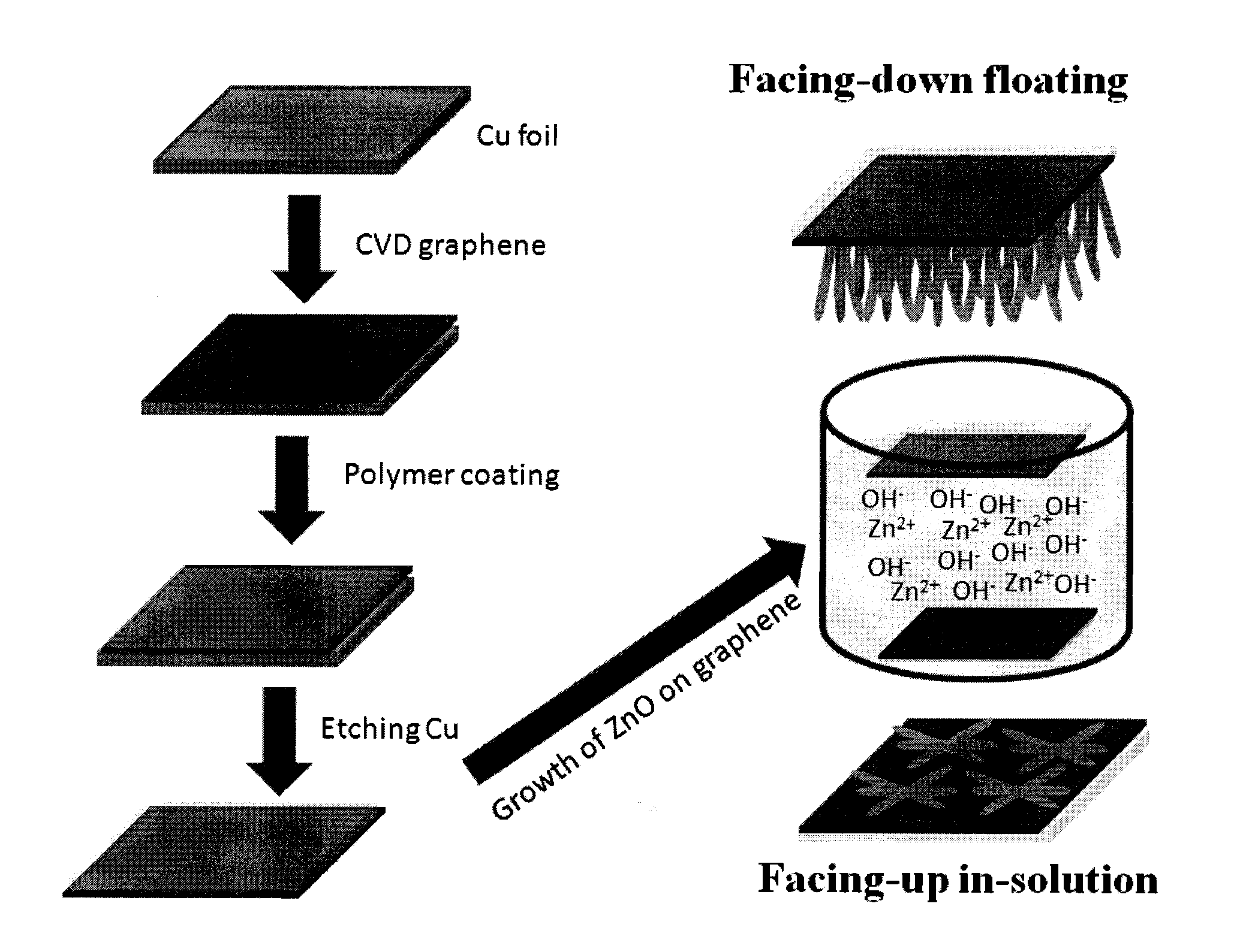
[0042]Synthesis of controlled aligned orientation of crystalline ZnO micro / nanowire on graphene sheets. FIG. 1 depicts respectively the facing-up in solution and facing-down floating growth processes for synthesis of the hybrid ZnO / graphene nanostructures. Graphene sheets were grown on Cu foils using CVD. PMMA was spin-coated on one side of the as-grown graphene before the sample was immersed into iron chloride solution (0.1 g / mL) for removal of the copper foil. After removing the Cu foil, the graphene sheets were either placed face-down or attached to a substrate for face-up in solution configuration for growth of ZnO micro / nanowires on graphene. For face-down floating growth of ZnO on graphene, the sample of PMMA / graphene floated on the surface of the solution during the entire procedure of the ZnO growth with graphene side facing down since the PMMA / graphene composite sample has a lower density than that of the solution. For face-up in solution, t...

example 2

Characterization of ZnO Graphene Hybrid Morphology

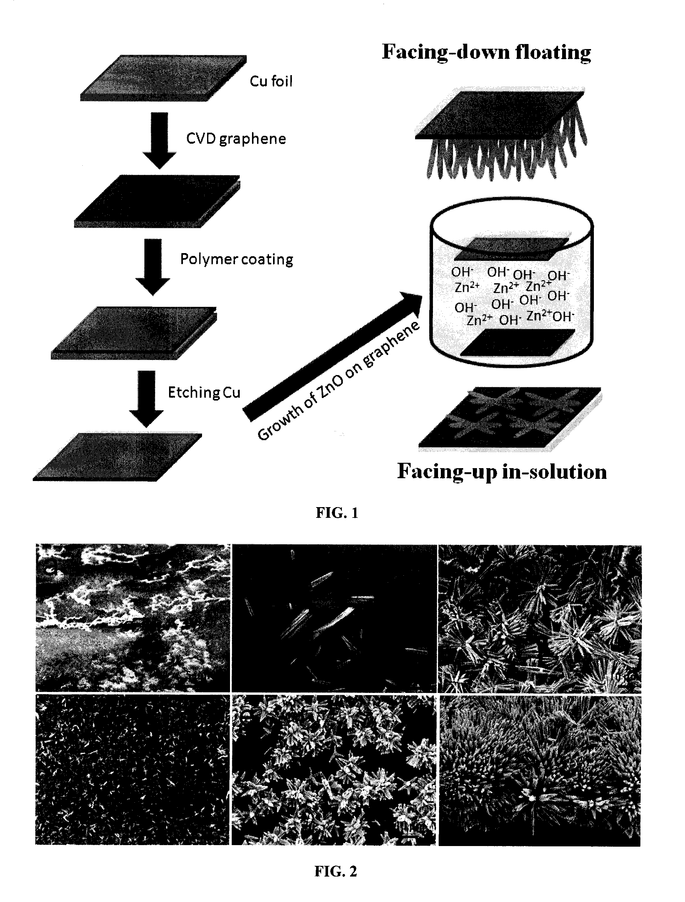
[0045]FIG. 2 includes the scanning electron microscopy (“SEM”) images of representative ZnO / graphene samples grown in solution for 3, 6, and 12 hours, respectively in the face-up (FIG. 2, panels a-c) and face-down floating configurations. After 3 hours solution growth, consideration differences can be observed in the two configurations. In the former, a substantial portion of the graphene surface area was covered with reaction residues or impurities (FIG. 2, panel a), which may prevent nucleation of ZnO directly on graphene. In fact, ZnO crystallites are barely observable in this case. In contrast, dense, uniform ZnO crystalline nanorods (see TEM data later for confirmation of the crystalline structures) were formed on graphene with negligible appearance of impurities in the latter configuration as shown in FIG. 2, panel d. The diameter of the ZnO nanorods is in the range of several to several tens of nanometers. This result suggests...

example 3

Crystal Structure of ZnO Graphene Hybrids

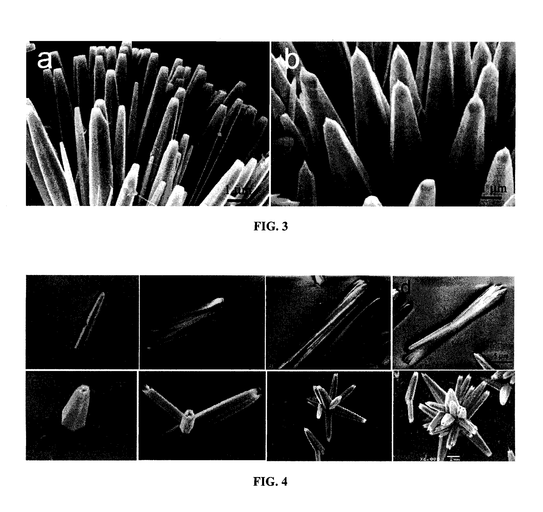
[0051]The crystal structure of the ZnO micro / nano-wires was characterized using X-ray diffraction (“XRD”) (Bruker SMART APEX). FIG. 7A shows the XRD θ-2θ patterns of a ZnO / graphene hybrid sample with 12 hour growth time. The diffraction peaks in FIG. 7A can be indexed to the wurtzite ZnO structure (JCPDS card no. 36-1451) and the lattice constants of this hexagonal phase are c0=5.21 Å and a0=3.25 Å, respectively (see Liu, et al. (2003)) The XRD diffraction peaks of (100), (002), and (101) are the most intensive ones. While (002) peak is expected for the c-axis oriented ZnO nano / micro-rods, the (100) and (101) peaks are also anticipated from the tilted ZnO nanowires as shown in panel f of FIG. 2. A further investigation on the ZnO micro / nano-wire microstructure using high-resolution transmission electron microscopy (“HRTEM”) (FIG. 7B) reveals the ZnO(0001) fringes perpendicular to the nanowire axis are on average separated by 0.26 nm, indicati...


PUM


Abstract

A novel method for fabrication of hybrid semiconductor-graphene nanostructures in large scale by floating graphene sheets on the surface of a solution is provided. Using this approach, crystalline ZnO nano/micro-rod bundles on graphene fabricated using chemical vapor deposition were prepared. UV detectors fabricated using the as-prepared hybrid ZnO-graphene nano-structure with graphene being one of the two electrodes show high sensitivity to ultraviolet light, suggesting the graphene remained intact during the ZnO growth. This growth process provides a low-cost and robust scheme for large-scale fabrication of semiconductor nanostructures on graphene and may be applied for synthesis of a variety of hybrid semiconductor-graphene nano-structures demanded for optoelectronic applications including photovoltaics, photodetection, and photocatalysis.

Description

CROSS-REFERENCE TO RELATED APPLICATIONS[0001]This application is based on and claims priority to U.S. Provisional Application Ser. No. 61 / 549,464, filed on Oct. 20, 2011, which is incorporated herein by reference in its entirety.STATEMENT REGARDING FEDERALLY SPONSORED RESEARCH OR DEVELOPMENT[0002]The present invention was sponsored by the U.S. Army Research Office Contract No. ARO-W911NF-09-1-0295 and W911NF-12-1-0412, and National Science Foundation Contracts Nos. NSF-DMR-0803149, 1105986, and EPSCoR-0903806, and the government may have certain rights in the invention.BACKGROUND OF THE INVENTION[0003]Graphene, a one-atom-thick planer sheet of sp2 bonded carbon atoms, holds promise for optoelectronic applications due to its unique properties of high carrier mobility at room temperature, with reported values in excess of 15,000 cm2V−1s−1, optical transmittance of about 97.9% for white light and flexibility (see Novoselov et al. (2005); Geim et al. (2007); and Novoselov et al. (2004))...

Claims


Application Information

Patent Timeline
IPC IPC(8): H01L21/36H01L29/06B82Y40/00
CPCH01L21/02376H01L21/02425H01L21/02527H01L21/02554H01L21/02603H01L21/02628H01L29/1606B82Y40/00H01L33/0087H01L33/18B82Y30/00H01L29/0676H01L21/02658Y10T428/30Y02E10/547H10N99/05B05D3/007B05D2201/06H01L31/022466H01L31/028H01L31/103
Inventor WU, JUDYLIU, JIANWEI
Owner UNIVERSITY OF KANSAS
Why Eureka
Try Eureka