Organic electroluminescent element, compounds and materials used for the organic electroluminescent element, and light-emitting, display and illuminating devices using the elements

Active Publication Date: 2013-08-22
UDC IRELAND
View PDF1 Cites 30 Cited by
  • Summary
  • Abstract
  • Description
  • Claims
  • Application Information

AI Technical Summary

Benefits of technology

[0015]According to the present invention, it is possible to provide an organic electroluminescent element

Problems solved by technology

However, studies conducted by the present inventors found that the organic electroluminescent elements described in Patent Documents 1 to 3 are unsatisfactory from the viewpoint of luminous efficiency.
However, Patent Documents 1 to 4, including Patent Document 3, neither disclose nor suggest how the luminance is deteriorated particularly at the initial light time.
As a result, it was noted that dissatisfaction remains from the viewpoint of a luminance deterioration rate at the initial stage of lighting.
However, it was noted that, for example, when such an element in which the luminance deterioration at the initial stage of

Method used


Image

  • Organic electroluminescent element, compounds and materials used for the organic electroluminescent element, and light-emitting, display and illuminating devices using the elements
  • Organic electroluminescent element, compounds and materials used for the organic electroluminescent element, and light-emitting, display and illuminating devices using the elements
  • Organic electroluminescent element, compounds and materials used for the organic electroluminescent element, and light-emitting, display and illuminating devices using the elements

Examples


example 1

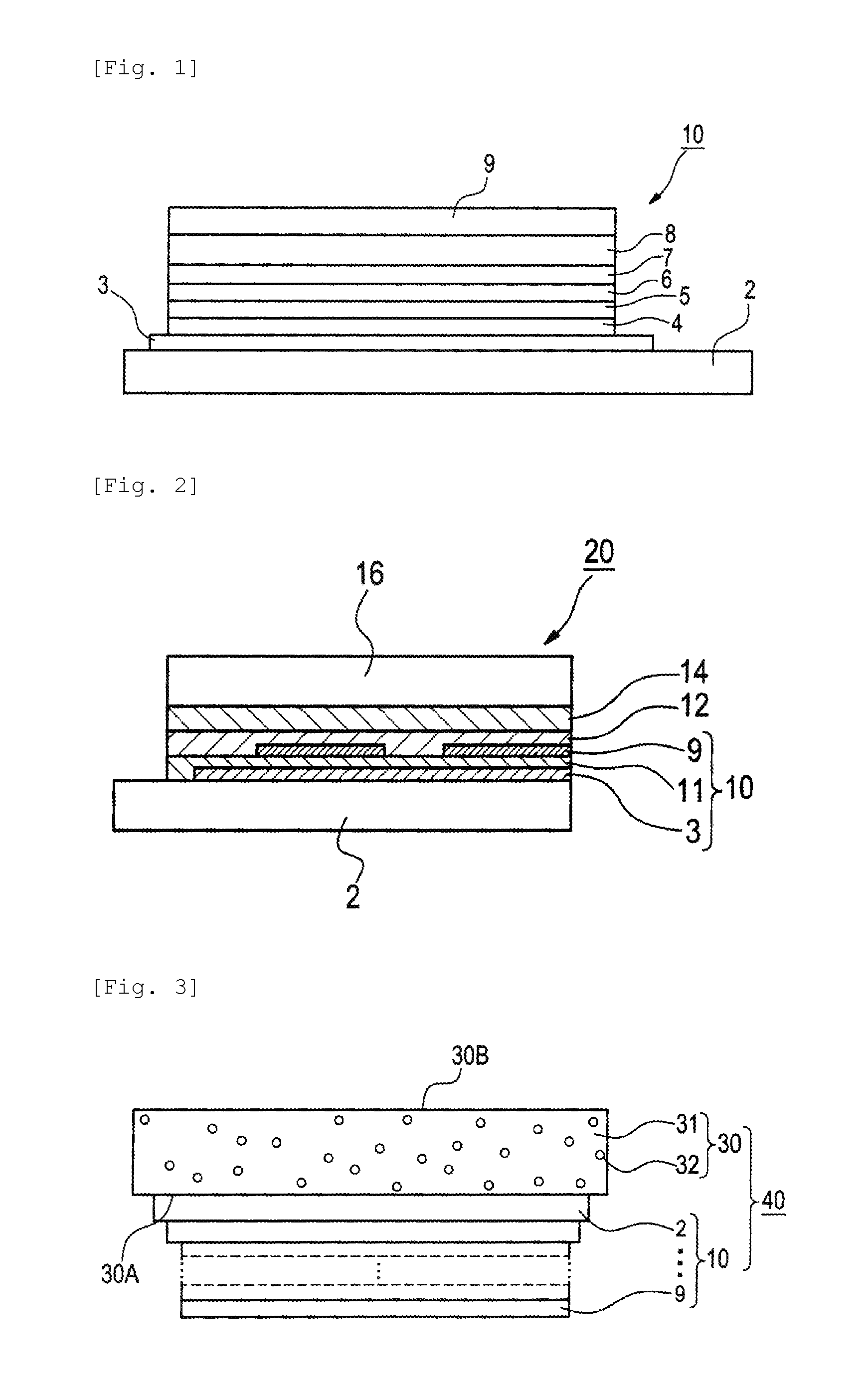
[0281]A compound (H-1) was synthesized according to the following scheme.

[0282]Sodium carbonate (171 g, 1.61 mol), 1-bromo-3-iodobenzene (77.3 mL, 806 mmol), toluene (400 mL), and water (800 mL) were charged into a 2-L three-neck flask, and were stirred at room temperature. The mixture was deaerated, and purged with nitrogen, and triphenylphosphine (21.2 g, 80.8 mmol), 4-biphenylboronic acid (80.0 g, 404 mmol), and palladium acetate (4.53 g, 20.2 mmol) were added. The reaction mixture was then refluxed and stirred under the nitrogen atmosphere for 7 hours. Then, the mixture was cooled to room temperature and ice-cooled. The precipitated solid was filtered, and washed with water and methanol to obtain compound 1 as a white solid (104 g).

[0283]The compound 1 (104 g, 336 mmol), bis(pinacolato) diboron (102 g, 402 mmol), potassium acetate (98.7 g, 1.01 mol), and anhydrous dimethylsulfoxide (1,000 mL) were added to a 2-L three-neck flask, and were stirred at room temperature. The mixture...

examples 2 to 11

[0288]The following compounds (H-2) to (H-14) were synthesized by using the same method used for the compound (H-1).

(Light Emitting Wavelength)

[0289]The compounds (H-1) to (H-14) of the present invention and compound D-2 (light emitting material; described later) were deposited on a quartz glass substrate (thickness: 0.7 mm, 2.5 cm square) in a 95:5 mass ratio by using a vacuum deposition method. As a result, a 50 nm-thick thin film was formed. The film was irradiated with 350-nm UV light, and the luminous spectrum of the emitted light was measured with a fluorescence spectrometer (JASCO Corporation; FP-6300) to read the maximum light emitting wavelength (nm).

[0290]Table 1 presents the results of the evaluation, using the following criteria.

Good: 435 nm or more and less than 455 nm

Acceptable: less than 435 nm

Poor: 455 nm or more

TABLE 1LightLight emittingemittingHost materialmaterialwavelengthRemarksCompound (H-1)Compound D-2GoodPresentinventionCompound (H-2)Compound D-2GoodPresentin...

example 101

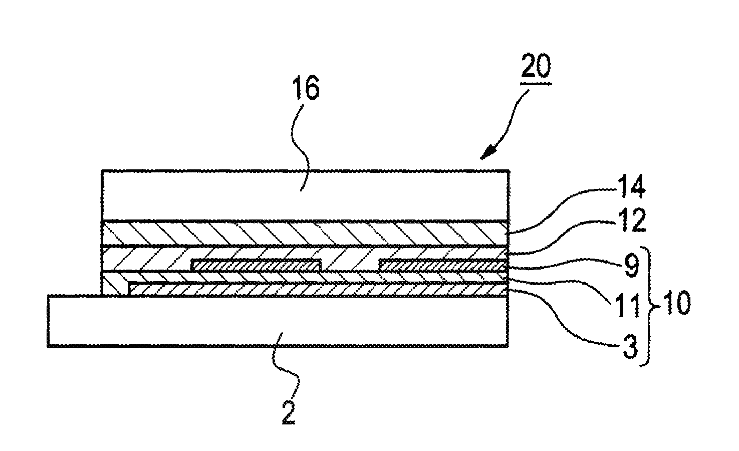
[0291]A glass substrate having an ITO film measuring 0.5 mm in thickness and 2.5 cm square in size (Geomatec Co., Ltd.; surface resistance 10Ω / □) was placed in a washing container. After ultrasonic washing in 2-propanol, the substrate was UV-ozone treated for 30 min. The following organic compound layers were deposited in order on the transparent anode (ITO film), using a vacuum deposition method.

First layer: HAT-CN; thickness 10 nm

Second layer: HTM-1; thickness 30 nm

Third layer: Compound (H-1) and compound (D-1) (mass ratio 95:5); thickness 30 nm

Fourth layer: ETM-1; thickness 30 nm

[0292]Then, lithium fluoride (1 nm) and metallic aluminum (100 nm) were deposited thereon in this order to make a cathode.

[0293]The resulting laminate was put in a glove box purged with a nitrogen gas without bringing it into contact with the atmosphere and then sealed with a sealing can made of glass and an ultraviolet ray-curable adhesive (XNR5516HV, manufactured by Nagase-CIBA Ltd.). As a result, organ...


PUM

PropertyMeasurementUnit
Currentaaaaaaaaaa
Digital informationaaaaaaaaaa
Electric chargeaaaaaaaaaa

Abstract

An organic electroluminescent element is provided that has high luminous efficiency, and a slow luminance deterioration rate in the initial stage of lighting. The organic electroluminescent element includes a substrate; a pair of electrodes including an anode and a cathode, disposed on the substrate; and at least one organic layer including a light emitting layer, disposed between the electrodes, wherein at least one organic layer includes a compound represented by the general formula (1). (R11 to R15 represent hydrogen atoms, alkyl groups, or silyl groups, and any one of R21 to R24 represents a group represented by general formula (1A) or (1B). Ph4 represents a p-phenylene group, and at least one of Ph4a and Ph4b represents a p-phenylene group.)

Description

FIELD OF THE INVENTION[0001]The present invention relates to organic electroluminescent elements, compounds usable therefor, and materials for organic electroluminescent element. The present invention also relates to light emitting devices, display devices, or illumination devices using the organic electroluminescent element.BACKGROUND OF INVENTION[0002]Since organic electroluminescent elements (which may hereinafter also be referred to as “elements” or “organic EL elements”) are capable of high-luminance light emitting using low voltage driving, they have been actively researched and developed. The organic electroluminescent elements have a pair of electrodes and an organic layer between the pair of electrodes, and utilize, for light emitting, energy of the exciton generated as a result of recombination of the electron injected from the cathode and the hole injected from the anode in the organic layer. The organic electroluminescent elements have potential application in a wide ran...

Claims


Application Information

Patent Timeline
IPC IPC(8): H01L51/00
CPCH01L51/0058C09B3/78H01L51/006H01L51/5012C07B2200/05C07C15/28C07C2103/24C09K11/06C09K2211/1011C09K2211/1014C09K2211/1044C09K2211/1059C09K2211/1088C09K2211/1092C07F7/0809C07F7/0818C09B57/00C09B57/001C09B57/008C09B1/00H01L51/0052C07C2603/24C07F7/081C07F7/0805H10K85/626H10K85/633H10K85/615H10K50/11
Inventor WATANABE, KOUSUKETAKAKU, KOJITOYAMA, WATARUISE, TOSHIHIROKINOSHITA, MASARUTAKADA, SAKI
Owner UDC IRELAND
Why Eureka
Try Eureka