

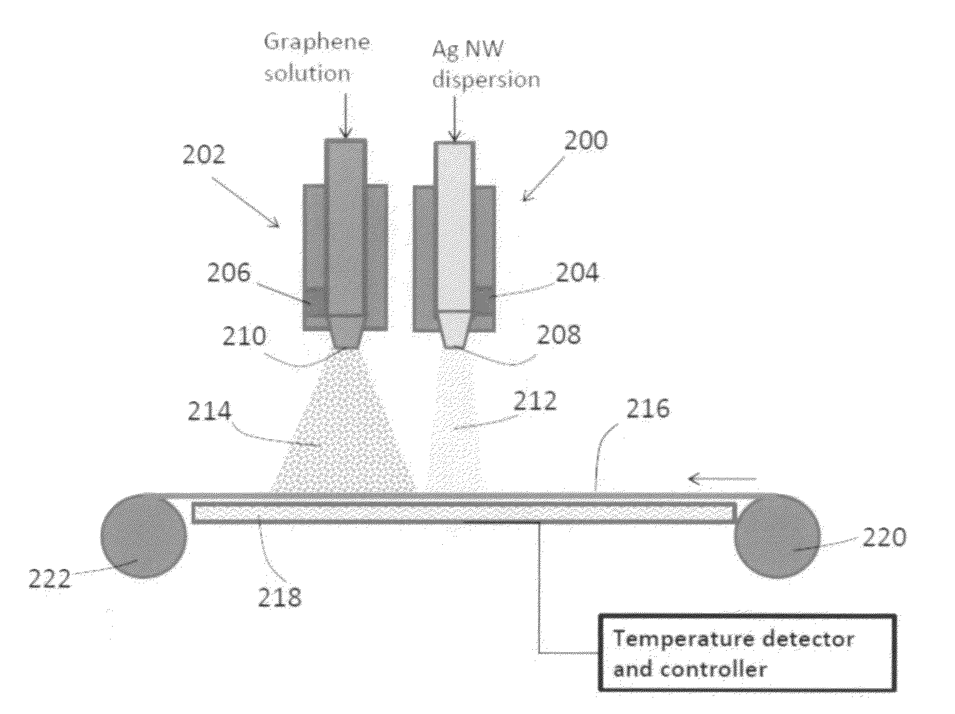
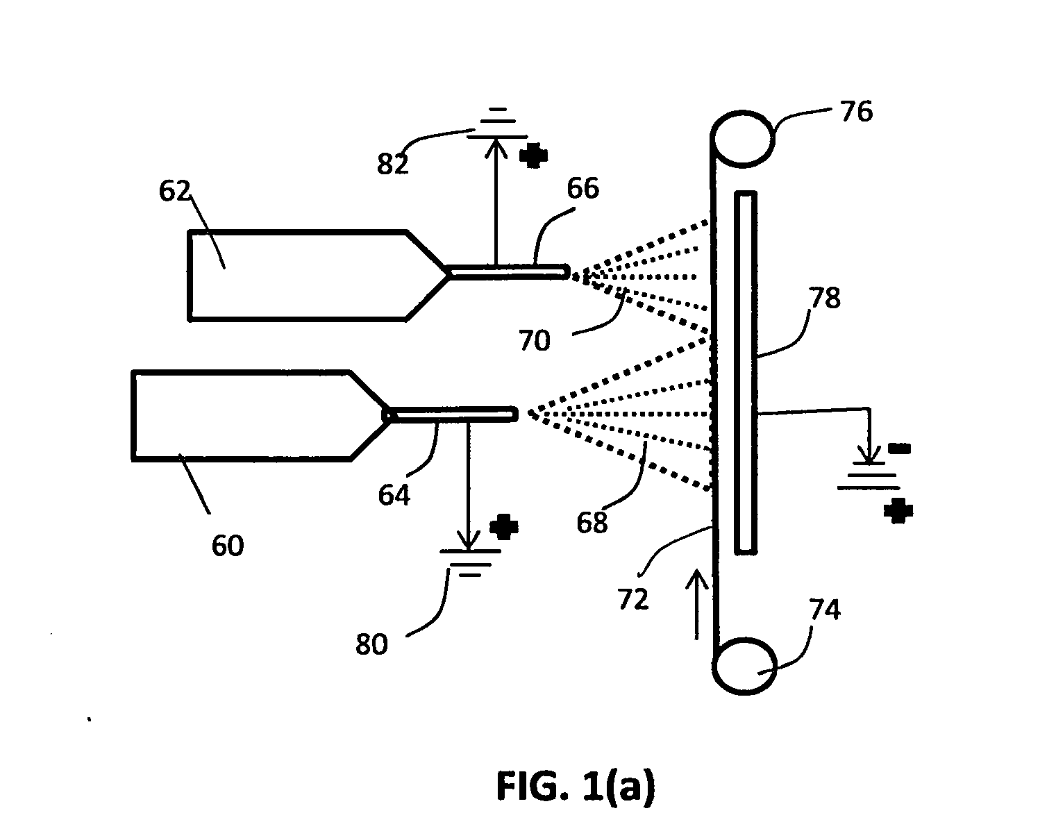
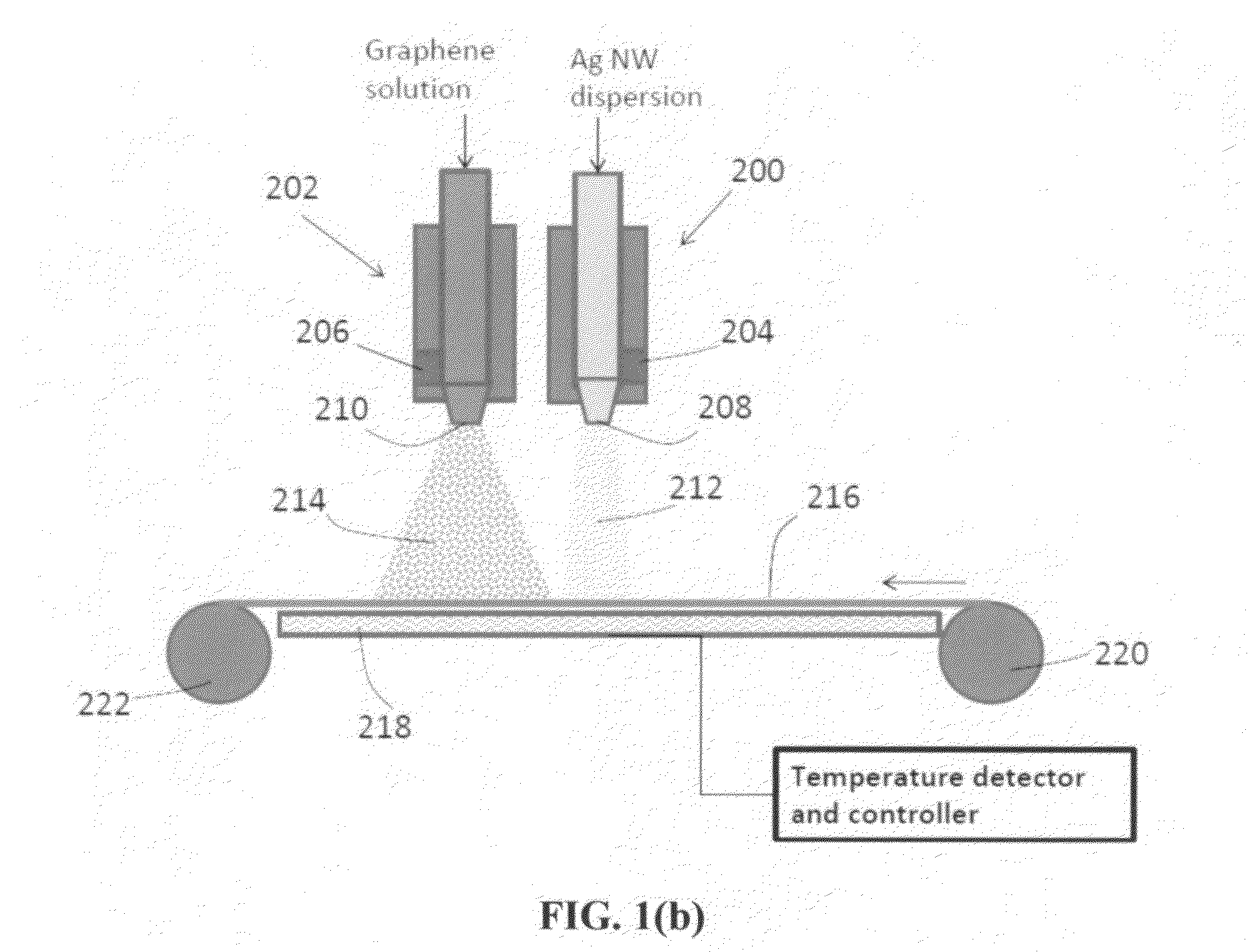
Ultrasonic spray coating of conducting and transparent films from combined graphene and conductive nano filaments
a nano-fibre and conducting technology, applied in the field of graphene/nano-based hybrid films, can solve the problems of high sheet resistance, 10-50 ohms/, and are not suitable for the practical application of transparent cnt electrodes in current-based devices, such as organic light-emitting diodes and solar cells. , to achieve the effect of reducing the resistance of the sheet, and high impingement speed
- Summary
- Abstract
- Description
- Claims
- Application Information
AI Technical Summary
Benefits of technology
Problems solved by technology
Method used
Image

Examples
example 1
Direct Ultrasonication Production of Pristine Graphene from Natural Graphite in a Low Surface Tension Medium
[0098]As an example, five grams of natural graphite, ground to approximately 20 μm or less in sizes, were dispersed in 1,000 mL of n-Heptane to form a graphite suspension. An ultrasonicator tip was then immersed in the suspension, which was maintained at a temperature of 0-5° C. during subsequent ultrasonication. An ultrasonic energy level of 200 W (Branson S450 Ultrasonicator) was used for exfoliation and separation of graphene planes from dispersed graphite particles for a period of 1.5 hours. The average thickness of the resulting pristine graphene sheets was 1.1 nm, having mostly single-layer graphene and some few-layer graphene.
example 2
Preparation of Pristine Graphene from Natural Graphite in Water-Surfactant Medium Using Direct Ultrasonication
[0099]As another example, five grams of graphite flakes, ground to approximately 20 μm or less in sizes, were dispersed in 1,000 mL of deionized water (containing 0.15% by weight of a dispersing agent, Zonyl® FSO from DuPont) to obtain a suspension. An ultrasonic energy level of 175 W (Branson S450 Ultrasonicator) was used for exfoliation, separation, and size reduction for a period of 1.5 hour. This procedure was repeated several times, each time with five grams of starting graphite powder, to produce a sufficient quantity of pristine graphene for thin film deposition.
example 3
Preparation of Pristine Graphene Using Supercritical Fluids
[0100]A natural graphite sample (approximately 5 grams) was placed in a 100 milliliter high-pressure vessel. The vessel was equipped with security clamps and rings that enable isolation of the vessel interior from the atmosphere. The vessel was in fluid communication with high-pressure carbon dioxide by way of piping means and limited by valves. A heating jacket was disposed around the vessel to achieve and maintain the critical temperature of carbon dioxide.
[0101]High-pressure carbon dioxide was introduced into the vessel and maintained at approximately 1,100 psig (7.58 MPa). Subsequently, the vessel was heated to about 70° C. at which the supercritical conditions of carbon dioxide were achieved and maintained for about 3 hours, allowing carbon dioxide to diffuse into inter-graphene spaces. Then, the vessel was immediately depressurized “catastrophically’ at a rate of about 3 milliliters per second. This was accomplished by...
PUM
| Property | Measurement | Unit |
|---|---|---|
| sheet resistance | aaaaa | aaaaa |
| impingement speed | aaaaa | aaaaa |
| impingement speed | aaaaa | aaaaa |
Abstract
Description
Claims
Application Information