Capacitor element

a technology of capacitor elements and dielectric layers, applied in capacitor electrodes, capacitor dielectric layers, electrolytic capacitors, etc., can solve the problems of many defects, current may flow, and the dielectric layer is not sufficiently dense film with a suitable thickness, etc., to achieve less leakage current, high capacitance, and high frequency range

Inactive Publication Date: 2015-07-09
SHOWA DENKO KK
View PDF9 Cites 1 Cited by
  • Summary
  • Abstract
  • Description
  • Claims
  • Application Information

AI Technical Summary

Benefits of technology

[0008]According to the production method of the present invention, a solid electrolytic capacitor element having a dielectric layer with a smooth surface composed of tungsten oxide can be produced. The capacitor element or capacitor of the present invention has a high capacitance in a high frequency range and less leakage current.
[0009]Although the reason why such an effect is obtained is not clear, the reason is considered as follows. That is, in the present invention, since the dielectric layer composed of tungsten oxide has a smooth surface, a monomer for conductive polymer, which is a raw material of a semiconductor layer, enters deep into pores of the anode body so that the pores are filled with a uniform conductive polymer, consequently realizing a high capacitance in a high frequency range and less leakage current.
[0010]Chemical conversion treatment of a sintered compact of tantalum powder, niobium powder, or aluminum powder in a chemical conversion liquid containing an oxidant (Patent Document 2) does not result in a phenomena in which the capacitance in a high frequency range is higher than that obtained by chemical conversion treatment in a chemical conversion liquid containing an electrolyte, such as phosphoric acid. Therefore, the effect of the present invention is so unique that it is obtained only when tungsten is used.

Problems solved by technology

This dielectric layer is not a sufficiently dense film with a suitable thickness, and seems to have many defects that electric current may flow when voltage is applied.
Moreover, as shown in FIG. 2, narrow pores 12 make it difficult to uniformly form a semiconductor layer deep in the pores, which may reduce the capacitance.

Method used


Image

  • Capacitor element
  • Capacitor element
  • Capacitor element

Examples


example 1

Production of Sintered Compact

[0044]A tungsten powder having a 50% particle size (D50) of 0.56 μm was mixed with 0.5% by mass of silicon powder having a 50% particle size (D50) of 1 μm, and the mixture was then allowed to stand for 30 minutes at 1,450° C. under vacuum. The mixture was returned to room temperature, and the block object was crushed by a hammer mill, thereby producing a granulated powder having a 50% particle size (D50) of 110 μm (range of particle size distribution: 26 μm-146 μm). Part of silicon was reacted with tungsten, and an alloy of tungsten silicide was present in the tungsten surface layer.

[0045]Compression bodies were produced from the granulated powder. When forming, tungsten wires (lead wires) having a diameter Φ of 0.29 mm were implanted. The compression bodies were put in a vacuum firing furnace, and fired at 1,500° C. for 20 minutes, thereby producing 10,000 sintered compacts with a size of 1.0 mm×1.5 mm×4.5 mm (each lead wire was implanted in the 1.0 mm...

examples 25 and 26

, and Comparative Examples 23 and 24

[0065]Solid electrolytic capacitor elements were obtained in the same manner as in Examples 11 and 12, and Comparative Examples 6 and 7, except that the chemical conversion liquid used in the second chemical conversion treatment was changed to aqueous solutions of the recipes shown in Table 2. The surface of the dielectric layers produced in Examples 25 and 26 was smooth, without sharp projections, salient striae, or cracks. The 120-Hz capacitance, 10-kHz capacitance, and leakage current of these elements were measured, and their average values were calculated. Table 2 shows the results.

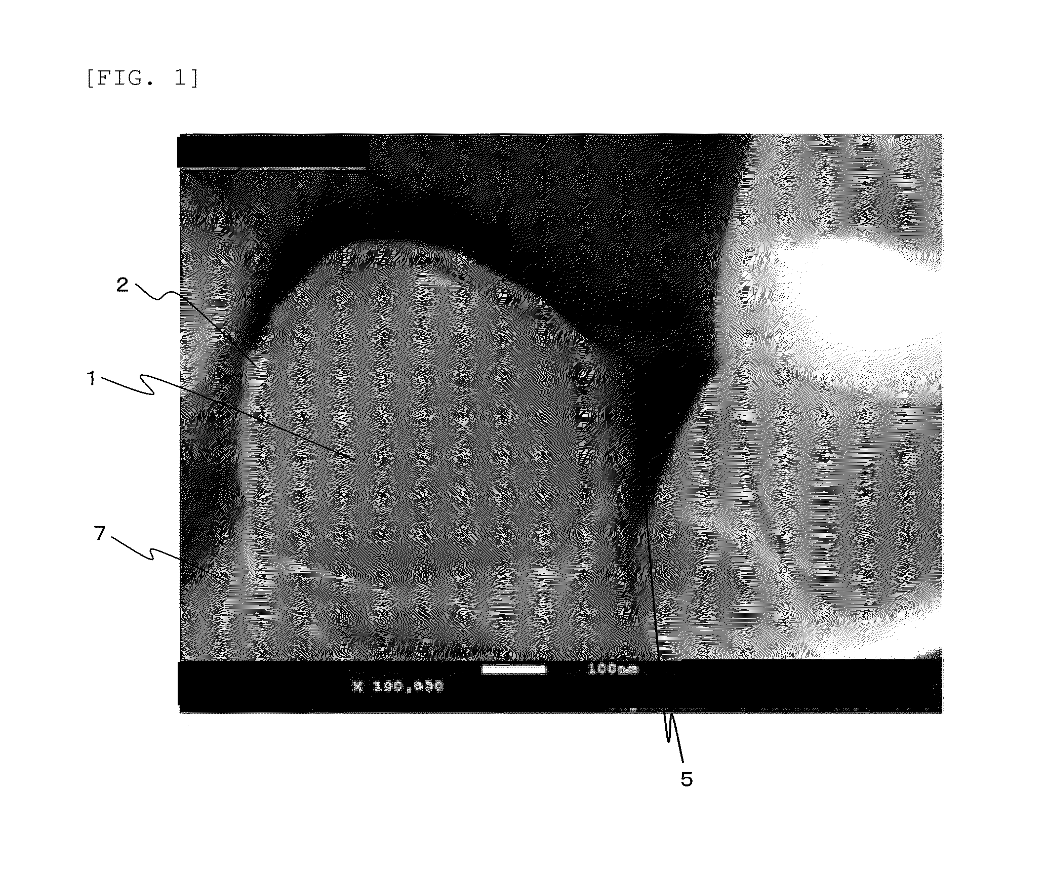
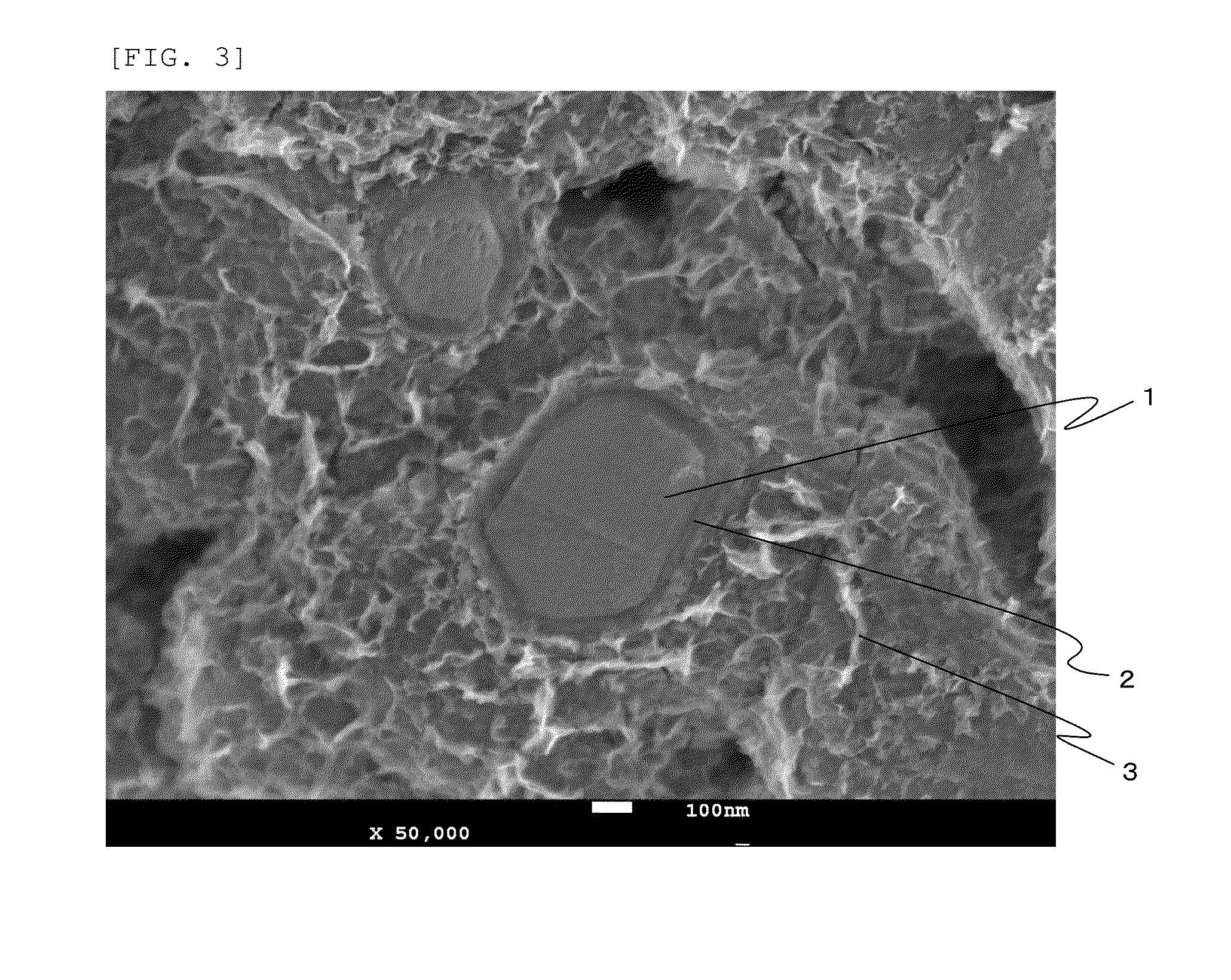
[0066]The surface of the dielectric layers produced in Comparative Examples 23 and 24 had pleat-like projections, as shown in FIG. 3. The 120-Hz capacitance, 10-kHz capacitance, and leakage current of these elements were measured, and their average values were calculated. Table 2 shows the results.

examples 29 to 31

[0071]Chemical conversion treatment was performed in the same manner as in Examples 3, 11, and 19, except that drying was performed without removing water with ethanol, while water remained in the pores, etc. Most of the obtained dielectric layers had a bluish-black smooth surface; however, 31 to 67 dielectric layers of the 128 dielectric layers were deteriorated, and the color of their outer surface was grayish-black. When the leakage current of the sintered compact having a grayish dielectric layer was measured in a 30% by mass sulfuric acid aqueous solution under conditions of room temperature, 2.5 V, and 30 seconds using the lead wire as positive electrode, and a platinum black plate placed in the liquid as negative electrode, the leakage current exceeded 100 μA.

[0072]When the leakage current of the sintered compact having a bluish dielectric layer was measured in a 30% by mass sulfuric acid aqueous solution under conditions of room temperature, 2.5 V, and 30 seconds using the l...


PUM

PropertyMeasurementUnit
temperatureaaaaaaaaaa

Abstract

A capacitor element including at least an anode body composed of a sintered compact containing tungsten as a main component, a dielectric layer with a smooth surface formed by chemical conversion of the surface of the anode body, and a semiconductor layer laminated on the dielectric layer. The capacitor is obtained by a production method which includes the steps of chemically converting the surface layer of the tungsten powder sintered compact into the dielectric layer in an aqueous solution containing 0.05 to 12% by mass of an oxidant composed of an oxygen-containing compound at a solution temperature of 62° C. or less, and removing all or most of water adhering to the inner surface of pores at a temperature of less than the boiling point of water, followed by drying at a temperature of not less than the boiling point of water.

Description

TECHNICAL FIELD[0001]The present invention relates to a capacitor element. More specifically, the present invention relates to a capacitor element that uses a tungsten anode body, and that has a high capacitance in a high frequency range and less leakage current.BACKGROUND ART[0002]Known capacitor elements are obtained by subjecting an anode body composed of a sintered compact of tantalum powder or niobium powder to electrolytic oxidation in an aqueous solution of an electrolyte such as phosphoric acid to chemically convert the surface layer of the sintered compact into a dielectric composed of metal oxide. Further, various techniques for improving tantalum capacitor elements have been proposed (Patent Document 2).[0003]Tungsten is known as one of valve action metals. When an anode body composed of a sintered compact of tungsten powder is subjected to electrolytic oxidation under the same conditions as the conditions of electrolytic oxidation of an anode body composed of a sintered ...

Claims


Application Information

Patent Timeline
Patent Type & Authority Applications(United States)
IPC IPC(8): H01G9/042H01G9/052H01G9/07H01G9/15
CPCH01G9/042H01G9/07H01G9/052H01G9/15H01G9/04
Inventor NAITO, KAZUMIYABE, SHOUJI
Owner SHOWA DENKO KK
Why Eureka
Try Eureka