Conductive nanocrystalline diamond micro-electrode sensors and arrays for in-vivo chemical sensing of neurotransmitters and neuroactive substances and method of fabrication thereof
a nano-crystalline diamond and nano-electrode technology, applied in the field of in-vivo chemical micro-sensors, can solve the problems of affecting the detection accuracy of neurotransmitters, so as to reduce fouling and tissue interaction, improve the sensitivity, and reduce the effect of sensitivity
- Summary
- Abstract
- Description
- Claims
- Application Information
AI Technical Summary
Benefits of technology
Problems solved by technology
Method used
Image
Examples
first embodiment
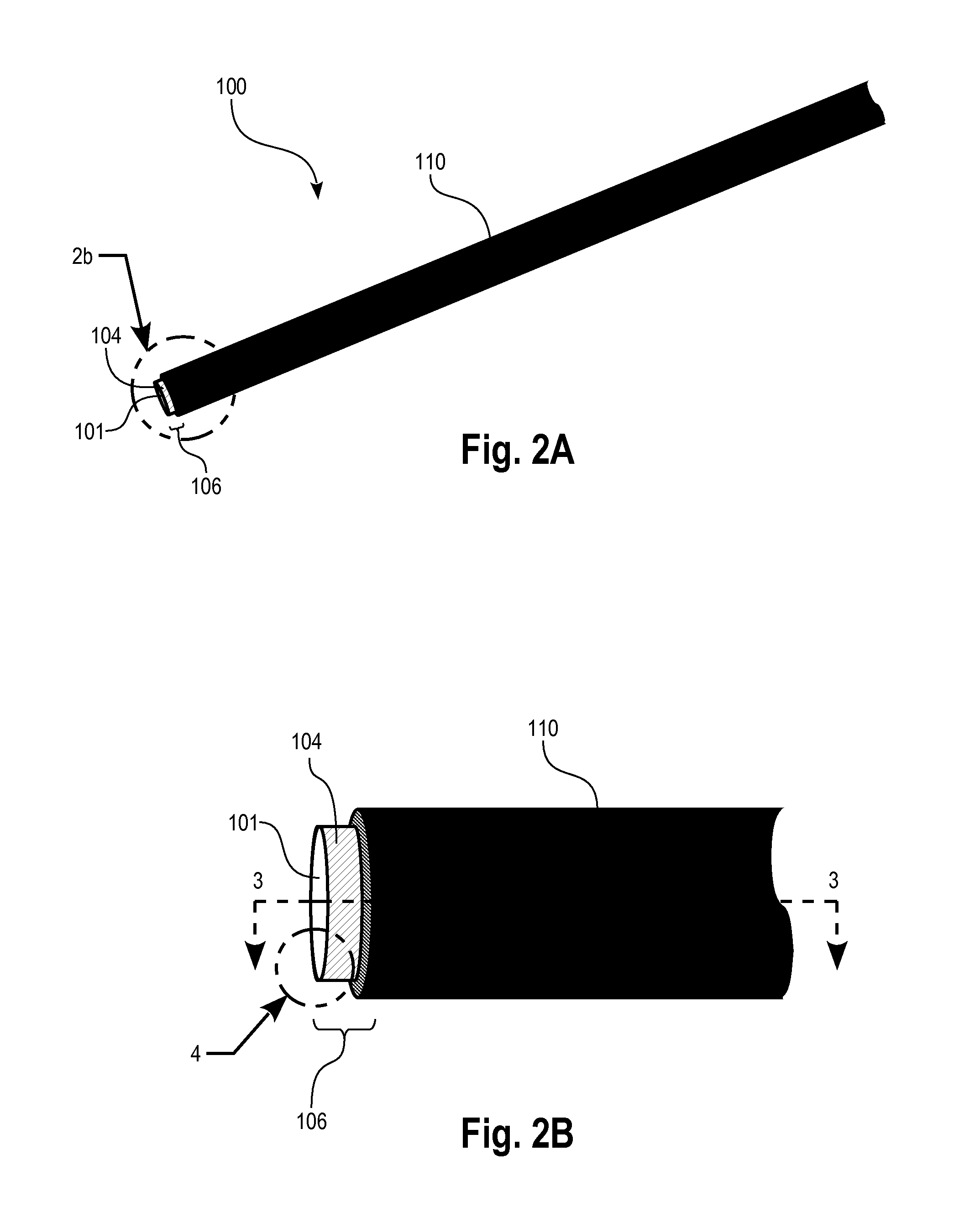
[0085]FIG. 2A illustrates schematically a micro-electrode sensor 100 or “probe” suitable for in vivo sensing of neurotransmitters. The sensor 100 comprises a conductive microwire 101, e.g. a metallic microwire of tungsten or other suitable metal, having a distal end portion which comprises a coating of conductive diamond, such as boron doped diamond (BDD), 104, defining sensor area 106 at the tip. The microwire is coated with a biocompatible insulating material 110, such as aluminum oxide or parylene, that has minimal reaction to the surrounding biomaterial in which it is implanted.
[0086]FIG. 2B illustrates schematically an enlarged view of the distal end portion showing the exposed conductive diamond sensor area 106. FIG. 3 illustrates a cross-sectional view of the sensor of FIGS. 2A and 2B. Preferably the conductive diamond layer is UNCD, which provides a sensor area having a very smooth surface, e.g. <10 nm rms surface roughness. As an example, the microwire may be fabricated ha...
second embodiment
[0088]FIG. 5 illustrates schematically a micro-electrode sensor 500 similar to that shown in FIGS. 2 and 3, but in which the end of the sensor tip 503 is coated with a layer conductive diamond which extends circumferentially around the cylindrical surface 501 beyond the insulating layer 110 and over the end 503 of the tip. The end coating 503 may provide further protection to the conductive microwire and in use, reduces the reactions of the microwire with the surrounding tissue.
third embodiment
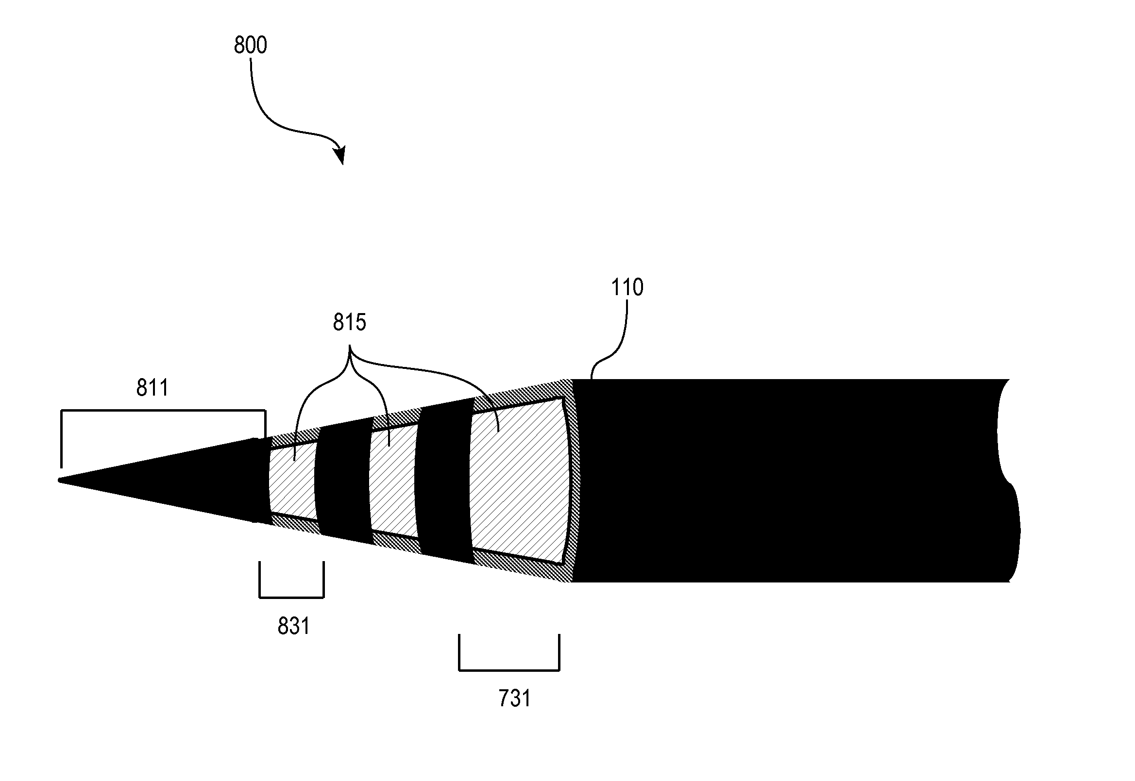
[0089]FIG. 6 illustrates schematically a micro-electrode sensor 600 comprising a tapered distal end portion 610 beyond the insulating layer 110, wherein the sensor area comprises a narrow or sharpened tip coated with UNCD. In some preferred embodiments, the microwire is sharpened to have a final tip point diameter of less than 2 μm or less than 1 μm. In use, tapering or sharpening the microwire to a fine point may reduce the interference of blood flow through capillaries in the test area. There may also be reduced damage to tissue and less interference to neuronal functions such as neurotransmitter release which is often caused by larger objects irritating the tissue.
[0090]The tip microwire is shaped or tapered, by conventional prior art etching or lapping, and then coated with the conductive diamond layer 611. For a simple structure where the entire tip forms a sensor area, the insulating material 110 may be selectively deposited on the microwire to leave the diamond tip exposed.
[...
PUM
| Property | Measurement | Unit |
|---|---|---|
| roughness | aaaaa | aaaaa |
| surface roughness | aaaaa | aaaaa |
| thickness | aaaaa | aaaaa |
Abstract
Description
Claims
Application Information


