Unlock instant, AI-driven research and patent intelligence for your innovation.

Systems and high throughput methods for touch sensors

Active Publication Date: 2016-09-29
WANG HAILIANG
View PDF5 Cites 33 Cited by
  • Summary
  • Abstract
  • Description
  • Claims
  • Application Information

AI Technical Summary

Benefits of technology

The patent describes a process for making a touch sensor that involves applying a layer of liquid encapsulation material to a protective film, curing it, and then peeling off the film to expose the touch sensor. This process provides a protective and secure way to encapsulate the touch sensor. The technical effect is to improve the reliability and durability of the touch sensor while maintaining its sensitivity.

Problems solved by technology

Every manufacturing step adds to the cost of the final device, due to materials used and elongated manufacturing time.
Since every step may have risks for causing defects, losses or decreasing production yield further contribute to the overall cost.
In addition, as the size of the capacitive touch screen increases, so does its weight since the typical touch screen comprises two layers of glass.
Particularly, ITO based transparent conducting film may not meet the requirement of new products where light weight and great readability is essential.
However, a number of challenges still exist before such an approach can meet full manufacturing specifications including optical / electrical properties and mechanical and environment stability.
Especially lack of an efficient manufacturing process with high throughput capacity is one important hurdle.
Sheet resistance, or electric conductivity of the film, is largely limited by the contact among individual wires.
In addition, adhesion of nanowire films to the transparent substrate may be weak due to weak molecular interaction between the metal wires and the transparent substrate, such as glass and polymer substrate.
Efforts to improve adhesion without sacrificing the conductivity are reported in literature without much success.
Although such approaches might partially solve the adhesion problem, the surface conductivity of nanowire film would be lost.
The second major challenge is the stability of the nanowire films, particularly that of films comprising silver nanowires.
Such overcoats might slow down the penetration of the pollutants to the silver nanowire film.
However, as the thickness of the overcoat increase, the surface conductivity of the nanowire would also be lost.
The third major challenge is related to the application of nanowire film.
However, because the overcoat layer is transparent, it may not be ablated by the laser to allow evaporation and thereby removal of silver from the coating.
Therefore most of the silver vapor formed by laser ablation may be trapped underneath the overcoat, leading to crosstalk of the patterned lines and device failure.
However, there are still significant technical barriers for in-cell and on-cell type touch screens.
For the on-cell type touch screens, the primary issue is the noise injected from the display module, such as liquid crystal display (LCD).
As the touch sensor is structured to be closer and closer to the thin film transistor (TFT) switching elements of LCD, this noise substantially grows.
In the case of in-cell type touch screen, the touch sensor is implemented within the TFT structure, which is complicated to manufacture, and therefore this type of touch screen is only used for a few high end applications today.
Achieving required sheet resistance with polymer film substrates is more difficult since the polymer films usually have lower thermal stability than the glass substrates.
Such a high sheet resistance and a low transparency may only find applications in small size touch sensors.
ITO coatings on PET films with sheet resistances lower than 50 ohm / square are rarely available and expensive.
However, it still faces a number of technical challenges.
These two features of glass lens pose processing difficulties during the process scale up for commercialization.
If the process scale up involves sputtering of an ITO layer on a large strengthened glass followed by patterning of the ITO layer, there may be substantial losses during cutting of the large strengthened glasses into small devices, decreasing the process yield.
If the process involves small pieces of the strengthened glass, the productivity may dramatically drop.
Any disruption in the conductive layer, at the frame to the glass transition regions, would cause device failures.
This process may therefore be unsatisfactory.

Method used


Image

  • Systems and high throughput methods for touch sensors
  • Systems and high throughput methods for touch sensors
  • Systems and high throughput methods for touch sensors

Examples


example 1

Preparation of a Transparent Conductive Electrode

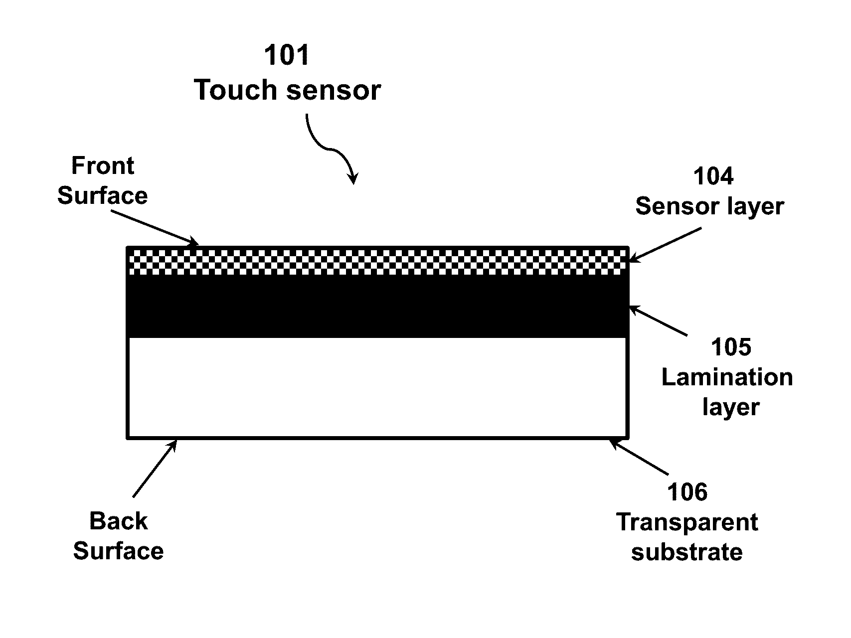
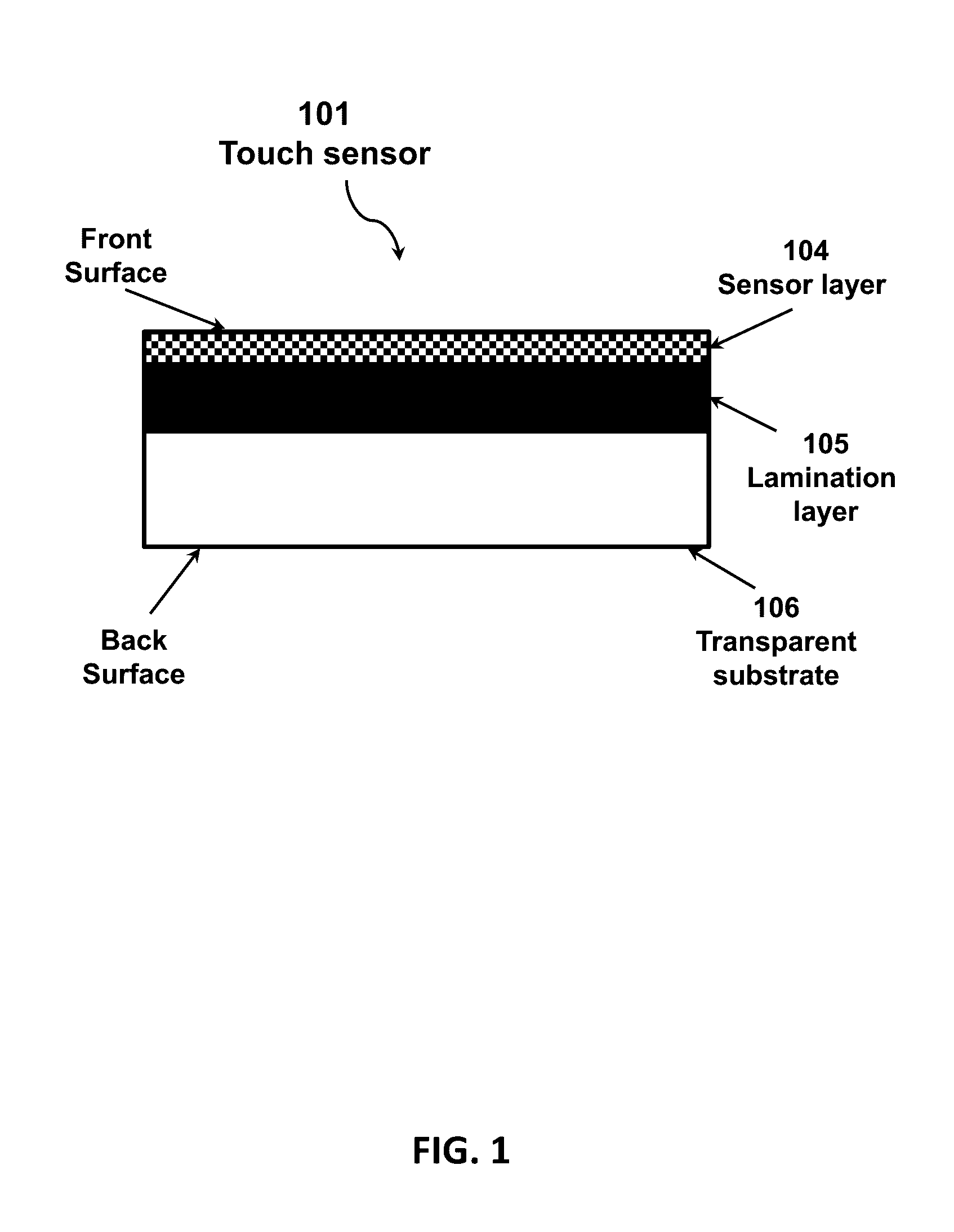
[0102]In this example, a method for preparation of a transparent conductive electrode is disclosed. This exemplary method is shown in FIGS. 6-8.

[0103]In this example, a protective film may be provided, as shown in FIG. 6. The protective film may be a film with a low coefficient of linear thermal expansion. The protective film may have a linear thermal expansion of less than 1.5% at 150 degrees centigrade, less than 0.8% at 150 degrees centigrade, or less than 0.5% at 150 degrees centigrade. The protective film may comprise any polymer (“the protective film polymer”). Examples of the protective film polymer may be poly (ethylene terephthalate) (PET), polycarbonate (PC), poly(ethylene naphthalate) (PEN), triacetylcellulose (TAC) and any combination thereof. Thickness of the protective film may vary in the range of 0.01 millimeter (mm) to 0.250 mm, or in the range of 0.01 mm to 0.150 mm.

[0104]In this example, a liquid formulation of the ...

example 2

Preparation of a Transparent Conductive Electrode

[0118]In this example, a method for preparation of a transparent conductive electrode is disclosed. This is a method alternative to that disclosed in Example 1. The formulations, the thermal and UV curing methods, and the coating methods used in this example are disclosed in Example 1 above. This exemplary method is shown in FIGS. 9-11.

[0119]In this example, the protective film is coated with the liquid nanomaterial dispersion. After the coating, the protective film may be thermally treated to remove the solvent and thereby to form a solid conductive nanomaterial layer on the surface of the protective film, as shown in FIG. 9-2A. A component 1 comprising the protective film and the conductive nano-material layer may thereby be prepared.

[0120]A “component 4” comprising the transparent substrate, the hard coat, the functional coating, and the liquid lamination layer may be prepared as follows, as shown in FIG. 10, 2B-2D. The component 4...

example 3

A High Throughput Preparation of a Transparent Conductive Electrode

[0122]In this example, a high throughput method for preparation of a transparent conductive electrode is disclosed. This exemplary method is shown in FIG. 12.

[0123]This method may use a first unwinding roll to release the protective film, a first slot die coater to coat the nanomaterial dispersion, a tunnel oven for the thermal treatment, a second slot die coater, a second unwinding roll for coating of the transparent substrate, a roll laminator and a UV curing system, and a rewinding roll.


PUM

PropertyMeasurementUnit
Timeaaaaaaaaaa
Angleaaaaaaaaaa
Angleaaaaaaaaaa

Abstract

This disclosure generally relates to an electronic system comprising a touch sensor and a method for manufacturing such system. This disclosure also generally relates to an electronic system comprising a transparent conductive electrode. This disclosure also generally relates to an optoelectronic system including a touch screen. This system may comprise a conductive nano-composite layer, a lamination layer, and a transparent substrate. The conductive nano-composite layer, the lamination layer, and the transparent substrate in combination may have optical transparency higher than 88% at about 550 nm, and sheet resistance lower than 45 ohms per square.

Description

BACKGROUND[0001]1. Technical Field[0002]This disclosure generally relates to an electronic system comprising a touch sensor and a method for manufacturing such system. This disclosure also generally relates to an electronic system comprising a transparent conductive electrode. This disclosure also generally relates to an optoelectronic system including a touch screen.[0003]2. Description of Related Art[0004]Since touch screens provide an easy interface for human-machine interactions, they recently have found wide range of applications in consumer electronics, such as mobile phones, tablets, global positioning systems (GPS), medical devices, laptops, point-of-sale terminals, point-of-information kiosks, industrial control units, and visual display systems.[0005]Among many types of the touch screens, capacitive touch screens are getting more popular as compared to resistive touch screens due to their higher sensitivity to finger touch and good visibility for displays. The capacitive t...

Claims


Application Information

Patent Timeline
IPC IPC(8): G06F3/044B32B27/08B32B38/10B32B27/30B32B27/28B32B37/12B32B7/12B32B27/36
CPCG06F3/044G06F2203/04103B32B27/08B32B27/365B32B27/308B32B27/281B32B37/12B32B38/10B32B2307/412B32B2457/208B32B2255/26B32B2264/108B32B2264/105B32B2255/10B32B2305/72B32B7/12B32B27/40B32B27/38B32B27/36B32B2307/202B32B2307/584B32B2307/554B32B2270/00B32B2307/734G06F3/0443
Inventor WANG, HAILIANG
Owner WANG HAILIANG
Features
  • R&D
  • Intellectual Property
  • Life Sciences
  • Materials
  • Tech Scout
  • Unparalleled Data Quality
  • Higher Quality Content
  • 60% Fewer Hallucinations
Learn More