A lithography composition, a method for forming resist patterns and a method for making semiconductor devices

Active Publication Date: 2019-12-12
MERCK PATENT GMBH
View PDF0 Cites 0 Cited by
  • Summary
  • Abstract
  • Description
  • Claims
  • Application Information

AI Technical Summary

Benefits of technology

[0024]Defects are reduced by using a present invention lithography composition. And a present invention lithography composition exhibits good performance for narrow pitched resist pattern rinsing, and can prevent pattern collapse

Problems solved by technology

Due to the high surface tension, pure water wash

Method used


Image

  • A lithography composition, a method for forming resist patterns and a method for making semiconductor devices
  • A lithography composition, a method for forming resist patterns and a method for making semiconductor devices
  • A lithography composition, a method for forming resist patterns and a method for making semiconductor devices

Examples


synthesis example 1

[0078]Following synthesis were done to obtain a novel compound represented by above formula (I)′ by the following synthesis scheme.

Potassium tert-Butoxide (Tokyo Kasei Kogyo Co Ltd.,) 7.4 g was dissolved in tert-butyl alcohol (Tokyo Kasei Kogyo Co Ltd.,) 100 g at room temperature in flask. Above Compound-1 (Unimatec Co Ltd.,) 6.5 g was added in flask by dropping funnel and it was stirred for 2 hour. After that, 1,3-Propanesultone (Tokyo Kasei Kogyo Co Ltd.,) 8.1 g in tert-butyl alcohol 10 g solution was added. And the solution was stirred at 65 degree for 6 hours. The solution was evaporated to remove the solvent. The rest material was dissolved in pure water 100 g. 36% HCl 40 g and Novec™7300 (by 3M) 50 g were added to the water solution. The Novec layer was taken and evaporated. And the above compound-2 was yielded (45%).

[0079]Known precursors and / or method can be combined above described synthesis example to obtain compound(s) that fall within formula (I)′. Those precursors can b...

synthesis example 2

[0080]Following synthesis were done to obtain a novel compound represented by above formula (I)′ by the following synthesis scheme

48% Potassium hydroxide water solution (Tokyo Kasei Kogyo Co Ltd.,) 200 g and Perfluoroethanesulfonamide (Penta ethane sulfone amide, Tokyo Kasei Kogyo Co Ltd.,) 150 g were mixed in flask. The salt solution was evaporated to remove water. The rest material 50 g and Compound-3 (Unimatec Co Ltd.,) 65 g was dissolved in Acetonitrile 200 g and stirred at 50 degree for 20 hours. The solution was filtrated and evaporated to remove Acetonitrile. The rest material was dissolved in water 200 g. 36% HCl 100 g and Novec™7300 (by 3M) 100 g were added to the water solution. The Novec layer was taken and evaporated. The compound-4 was obtained in a yield of 20%.

[0081]Known precursors and / or method can be combined above described synthesis example to obtain compound(s) fall within formula (I)′. Those precursors can be obtained by for example Unimatec Co. Ltd., or fluoro...

example 1

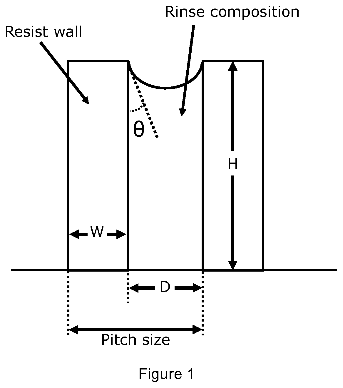
[0082]For a pattern collapse prevention performance evaluation, below procedures were done.

A Silicon wafer (SUMCO, 12 inch) surface was treated by a 1,1,1,3,3,3-Hexamethyldisilazane (HMDS) at 90 degree for 60 seconds. Chemical amplify PHS acrylate hydrate hybrid EUV resist was spin-coated on the silicon wafer, and soft-baked at 110 degree for 60 seconds to form a resist film in 50 nm thickness. The resist film on the wafer was exposed to light with varying the exposure dose through 20 nm size (line:space=1:1) mask in the EUV exposure apparatus (High NA Small Field Exposure Tool, NA=0.51, quadrupole). The wafer was post exposure baked (PEB) 110 degree for 60 seconds. And the resist film was paddle-developed with 2.38% Tetramethylammonium Hydroxide (TMAH) aqueous solution for 30 seconds. Rinse water was poured into a puddle of the developer on the wafer, pouring thereof was continued while rotating the wafer to replace the developer with the rinse water, and the rotation of the wafer ...


PUM


Abstract

The present invention relates to a new lithography composition, the forming of resist patterns using the lithography composition, and a semiconductor device manufacturing method using the lithography composition in a photolithography method.

Description

TECHNICAL FIELD[0001]The present invention relates to a lithography composition and a method for forming a photoresist pattern using the lithography composition. One embodiment of the present invention relates to a lithography composition which can be used in a rinse process after development of a photosensitive resin composition applied for manufacturing of a semiconductor device, a flat panel display (FPD) such as a liquid crystal display element, a color filter and so on and to a method for forming a photoresist pattern. Another embodiment of the present invention relates to a semiconductor manufacturing method that includes a resist pattern rinse process using the lithography composition.BACKGROUND[0002]In various fields such as manufacturing of semiconductor integrated circuits for example a Large Scale Integration (LSI), display faces of flat panel displays (FPDs), circuit substrates, color filters, and so on, photolithography technology has so far been employed for conducting...

Claims


Application Information

Patent Timeline
IPC IPC(8): G03F7/40H01L21/027
CPCG03F7/322G03F7/162H01L21/0274G03F7/168G03F7/38G03F7/2004G03F7/40G03F7/425C11D11/0047C11D1/004C11D1/06C11D1/08C11D3/48G03F7/2012G03F7/32G03F7/70925G03F7/70033H01L21/027
Inventor YAMAMOTO, KAZUMAISHII, MAKIYASHIMA, TOMOYASUNAGAHARA, TATSURO
Owner MERCK PATENT GMBH
Why Eureka
Try Eureka