Composition for electronic devices, ink for electronic devices, and method for producing electronic device

a technology for electronic devices and inks, applied in the direction of luminescent compositions, coatings, inks, etc., can solve the problems of low device performance, solvents tend to remain in the film without volatilizing, and the material use efficiency is not suitable for mass production, so as to achieve high liquid stability and device performance, high device performance

Pending Publication Date: 2021-01-14
KONICA MINOLTA INC
View PDF1 Cites 0 Cited by
  • Summary
  • Abstract
  • Description
  • Claims
  • Application Information

AI Technical Summary

Benefits of technology

[0009]According to the above-mentioned means of the present invention, it is possible to provide a composition for an electronic device in which the residual amount of a solvent containing a fluorine-containing solvent in a formed film is reduced and the influence of the residual solvent on the device may be suppressed to exhibit high device performance, and to provide an ink for an electronic device and a method for manufacturing an electronic device in which the composition for an electronic device contains the composition, which have wet process suitability and exhibits high liquid stability and device performance.

Problems solved by technology

Since the dry process is the preparation of the device performed by vacuum deposition, while it is advantageous that it is easy to laminate a plurality of layers, the material use efficiency is not suitable for mass production.
However, since the fluorine-containing solvent has a very strong dipole interaction derived from the high electronegativity of fluorine, there has been a disadvantage that the solvent tends to remain in the film without volatilizing by interacting with the solute.
Therefore, there is a problem that the residual solvent lowers the device performance.

Method used


Image

  • Composition for electronic devices, ink for electronic devices, and method for producing electronic device
  • Composition for electronic devices, ink for electronic devices, and method for producing electronic device
  • Composition for electronic devices, ink for electronic devices, and method for producing electronic device

Examples


example 1

[0316]In Example 1, a thin film was formed from the composition for an electronic device of the present invention, and the residual amount of the fluorine-containing solvent was evaluated.

[0317]A quartz substrate having a length of 10 mm, a width of 10 mm, and a thickness of 0.7 mm was ultrasonically cleaned with isopropyl alcohol, dried with dry nitrogen gas, and UV ozone cleaning was performed for 5 minutes.

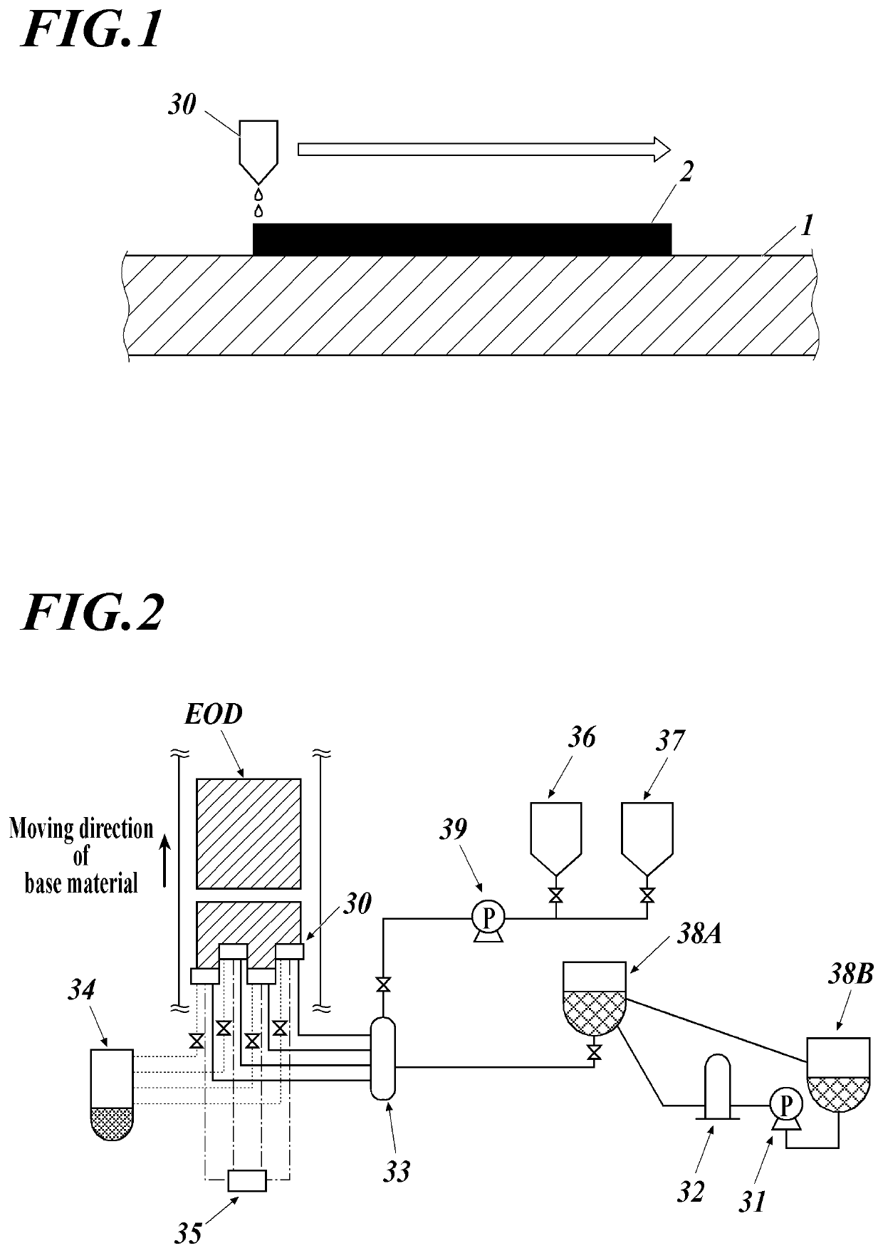
[0318]Compound B1 was dissolved in the solvent TFPO at a concentration of 1 mass % in a nitrogen-atmosphere as a component A. The obtained TFPO solution was used as an ink to form a 50 nm-thick film on the quartz substrate by an inkjet printing method shown in FIG. 1 and FIG. 2, and the quartz substrate was dried at 120° C. for 30 minutes in a nitrogen-gas atmosphere to form an evaluation monolayer 1-1.

[0319]The evaluation monolayer 1-2 was formed in the same manner as used for the formation of the evaluation monolayer 1-1 except that Compound B1 was replaced with Compound B2 a...

example 2

[0325]In Example 2, the drive voltage of a single-charge device (abbreviated as an electron-only device (EOD)) in which a coating film formed using a composition containing a π-conjugated boron compound and a fluorine-containing solvent according to the present invention was incorporated was evaluated.

(Formation of Anode)

[0326]On a glass substrate having a length of 50 mm, a width of 5 0 mm, and a thickness of 0.7 mm, ITO (indium tin oxide) was formed to a thickness of 120 nm and patterned to form an anode made of an ITO transparent electrode. Thereafter, ultrasonic cleaning was performed with isopropyl alcohol, dried with dry nitrogen gas, and UV ozone cleaning was performed for 5 minutes.

(Formation of Hole Blocking Layer)

[0327]Next, the substrate on which the anode was formed was fixed to a substrate holder of a commercially available vacuum deposition apparatus.

[0328]A resistance heating boat for deposition in the vacuum deposition apparatus was filled with an optimal amount of c...

example 3

[0337]In Example 3, the stability of a composition for an electronic device containing a π-conjugated boron compound, a fluorine-containing solvent, and a component C according to the present invention was evaluated.

[0338]After heating at 85° C. for 15 minutes in a nitrogen atmosphere, the mixture was returned to room temperature to prepare the following evaluation composition 3-1.

(Evaluation Composition 3-1)

[0339]Compound B6: 10 parts by mass

[0340]HFBO: 2000 parts by mass

[0341]The evaluation composition 3-2 was prepared in the same manner as used for the preparation of the evaluation composition 3-1 except that Compound B6 was replaced with Compound B7, and HFBO was replaced with TFPO.

[0342]Furthermore, the evaluation compositions 3-3 to 3-25 were prepared in the same manner as used for the preparation of the evaluation composition 3-2 except that Compound B7 and TFPO were replaced with the compounds or solvents listed in Table II. When there were a plurality of compounds, the tota...


PUM

PropertyMeasurementUnit
structureaaaaaaaaaa
Hansen solubility parameter distanceaaaaaaaaaa
compositionaaaaaaaaaa

Abstract

The present invention addresses the problem of providing: a composition for electronic devices in which when a film is formed therefrom, the amount of residual solvents including fluorine-containing solvents within the film is reduced, the effects of residual solvents on a device are minimized, and it is thus possible to achieve high element performance; an ink for electronic devices that is suitable for wet processes and that makes it possible to achieve high liquid stability and element performance as a result of containing the composition for electronic devices; and a method for producing an electronic device. This composition for electronic devices contains a component A and a component B and is characterized in that the component A is a fluorine-containing solvent and the component B is a compound having a structure represented by general formula (1).

Description

TECHNICAL FIELD[0001]The present invention relates to a composition for an electronic device, an ink for an electronic device, and a method for manufacturing an electronic device. More particularly, the present invention relates to a composition for an electronic device in which the residual amount of a solvent containing a fluorine-containing solvent in a formed film is reduced, and the influence of the residual solvent on the device may be suppressed to exhibit high device performance, and an ink for an electronic device and a method for manufacturing an electronic device in which the composition for the electronic device contains the composition for a wet process suitability and may exhibit high liquid stability and device performance.BACKGROUND[0002]When manufacturing an electronic device such as an organic electroluminescence element (hereinafter referred to as an organic EL element), an organic thin film solar cell, or an organic transistor, two manufacturing methods are used:...

Claims


Application Information

Patent Timeline
Patent Type & Authority Applications(United States)
IPC IPC(8): B41J2/01H01L51/00
CPCB41J2/01H01L51/5072H01L51/008C09D11/36C09D11/38C09K11/06H05B33/10H10K71/135H10K71/15H10K85/615H10K85/655H10K85/631H10K85/654H10K85/6574H10K85/322H10K50/165H10K50/18H10K50/16C09D7/20
Inventor KIMURA, AKIHIROOKANIWA, MIYUKIITO, HIROTO
Owner KONICA MINOLTA INC
Why Eureka
Try Eureka