Ultra-fine nanocrystalline diamond precision cutting tool and manufacturing method therefor
a nanocrystalline diamond and precision cutting technology, applied in the field of ultra-fine nanocrystalline diamond precision cutting tools and manufacturing methods therefor, can solve the problems of limiting the maximum cutting performance and use performance bursting and failing of single crystal diamond, and poor wear resistance of polycrystalline diamond, etc., to achieve high hardness, simple and effective, and strong toughness
- Summary
- Abstract
- Description
- Claims
- Application Information
AI Technical Summary
Benefits of technology
Problems solved by technology
Method used
Image
Examples
example 1
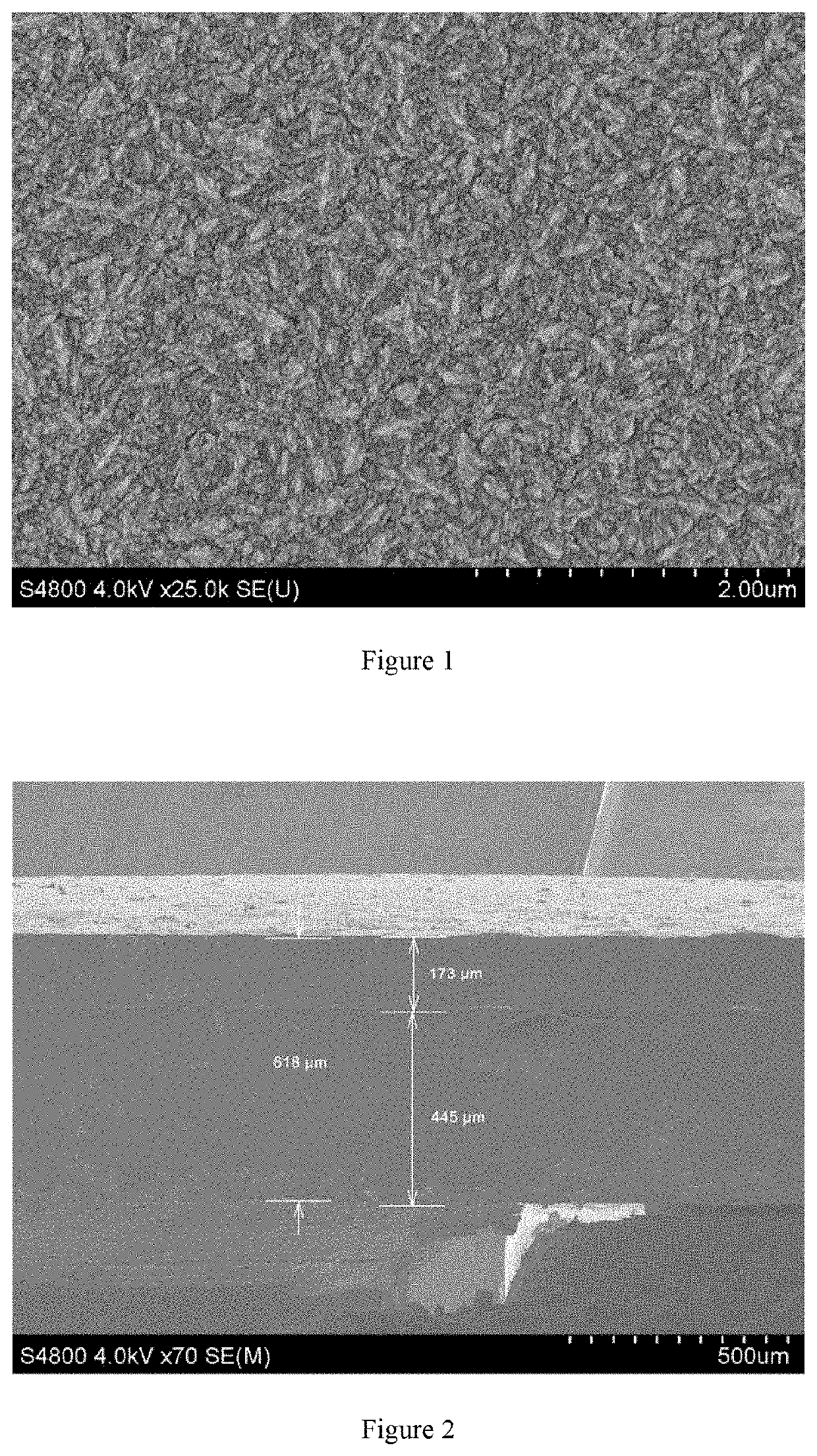
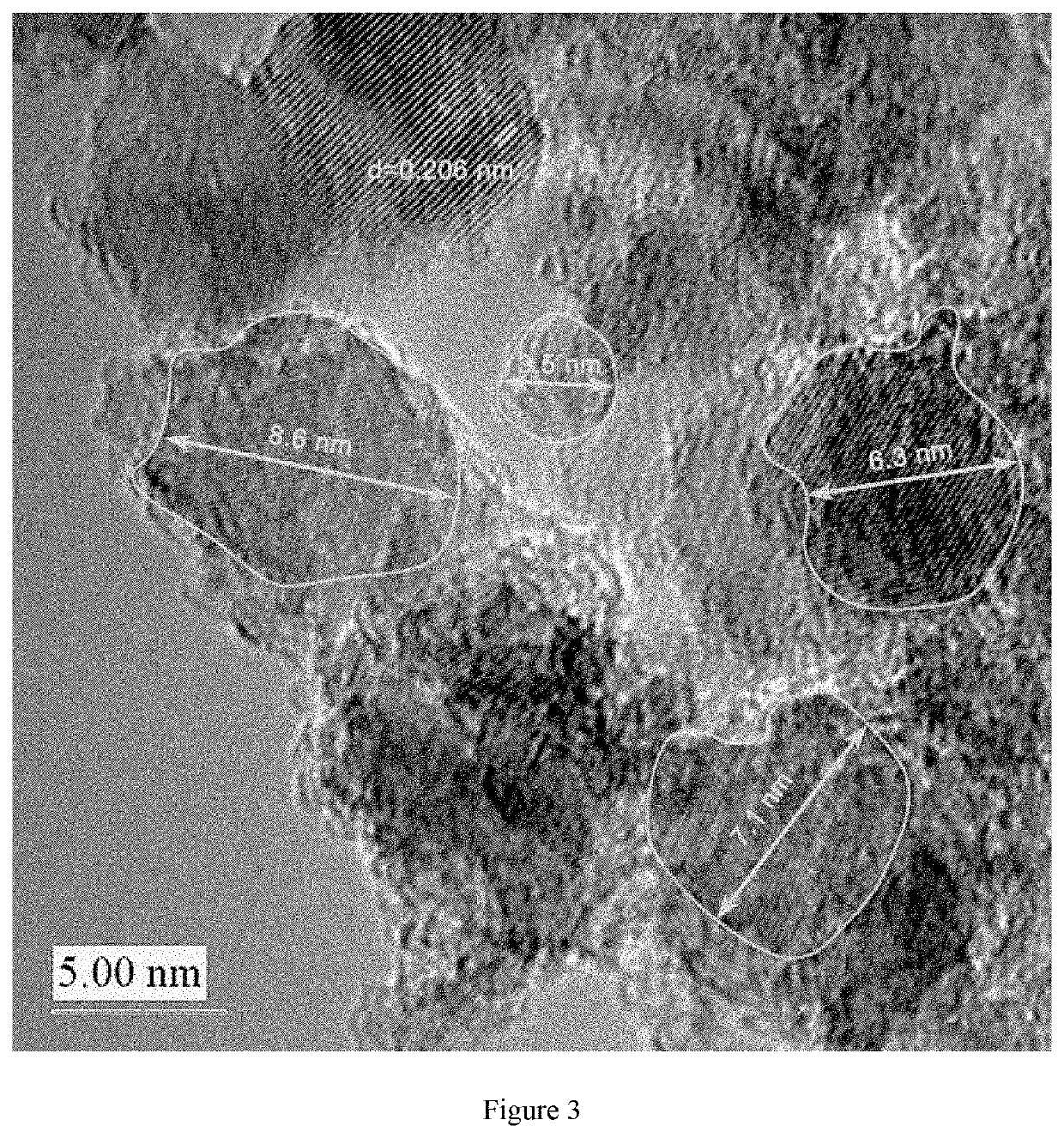
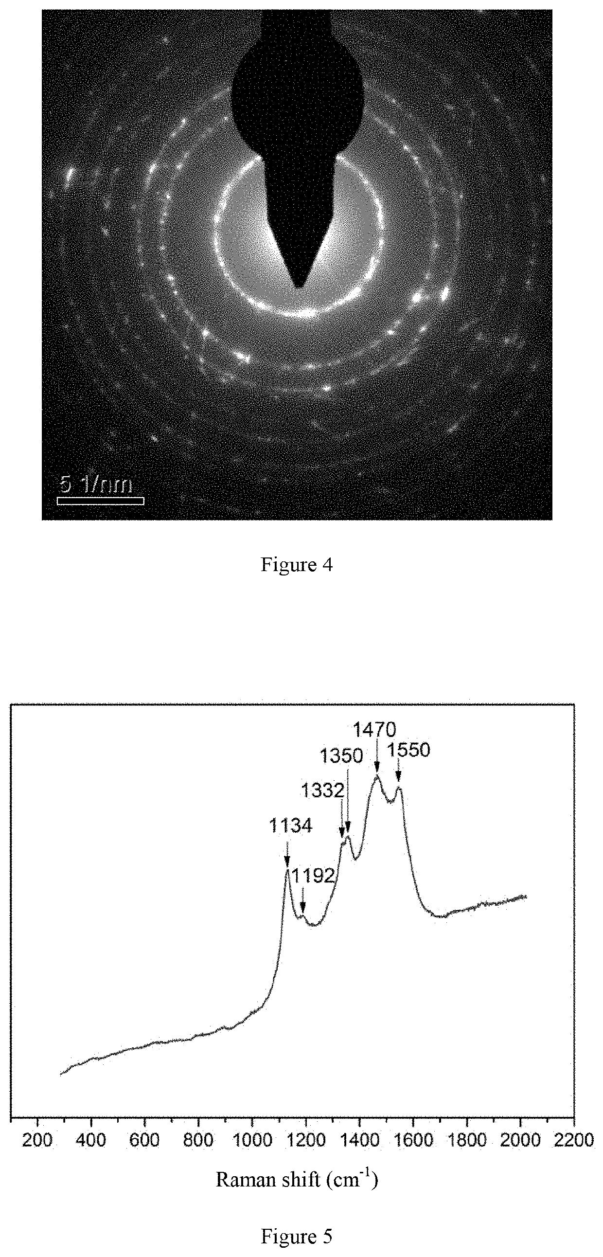
[0066]A silicon (100) surface with a diameter of 50-100 mm and a thickness of 500-3000 μm was used for chemical vapor deposition of ultra-fine nanocrystalline diamond thick film. Before being deposited, in order to increase the nucleation density of diamond to grow ultra-fine nanocrystalline diamond, the silicon wafer was ground with ultra-fine nanocrystalline diamond powder to form many nanogrooves on the surface of the silicon wafer to promote diamond nucleation. The ultra-fine nanocrystalline diamond powder had a particle size of 5-15 nm, and the silicon wafer was ground by hand grinding. The ground silicon wafer was ultrasonically cleaned with deionized water, then it was subjected to ultrasonic treatment in an alcohol suspension containing ultra-fine nanocrystalline diamond powder, and seeding was performed on the surface of the silicon. The ultrasound time was 5-30 min. High density ultra-fine nanocrystalline diamond powder was remained on the surface of the silicon wafer ultr...
example 2
[0086]A self-supporting ultra-fine nanocrystalline diamond thick film was prepared by using the method of Example 1, except that the distance between the hot filament and the sample was 14 mm, the growth pressure was 1.5 kPa, the concentration of methane was 2%, the concentration of inert gas was 10%, and the growth time of ultra-fine nanocrystalline diamond thick film was 30-1000 hours. As measured, the thickness of the thick film was 500 μm, and the average diamond grain size was 10 nm.
[0087]After cutting, welding and grinding, the manufacture of ultra-fine nanocrystalline diamond precision cutting tool was finished.
[0088]FIG. 11 is a scanning electron micrograph of the plan of the ultra-fine nanocrystalline diamond thick film obtained in example 2. It can be seen from FIG. 11 that the crystal grains of the diamond thick film are still ultra-fine nanocrystals. Compared with Example 1, the needle-like clusters were more obvious.
[0089]FIG. 12 is a Raman spectrum diagram of the ultra...
example 3
[0090]A self-supporting ultra-fine nanocrystalline diamond thick film was prepared by using the method of Example 1, except that the distance between the hot filament and the sample was 15 mm, the growth pressure was 1.5 kPa, the concentration of methane was 2%, the concentration of inert gas was 10%, and the growth time of ultra-fine nanocrystalline diamond thick film was 30-1000 hours. As measured, the thickness of the thick film was 450 μm, and the average diamond grain size was 12 nm.
[0091]After cutting, welding and grinding, the manufacture of ultra-fine nanocrystalline diamond precision cutting tool was finished.
[0092]FIG. 13 is a scanning electron micrograph of the plan of the ultra-fine nanocrystalline diamond thick film obtained in example 3. It can be seen from FIG. 13 that the crystal grains of the diamond thick film are still ultra-fine nanocrystals. Compared with Example 1, the diamond grains were no longer distributed in needle-like clusters.
[0093]FIG. 14 is a Raman sp...
PUM
| Property | Measurement | Unit |
|---|---|---|
| Temperature | aaaaa | aaaaa |
| Fraction | aaaaa | aaaaa |
| Fraction | aaaaa | aaaaa |
Abstract
Description
Claims
Application Information


