Many of these advances have been made possible through improvements
in process control since the conditions under which desired structures are formed may adversely affect previously formed structures.
However, further heat treatment subsequent to annealing may cause further
diffusion which is not desired.
The integrity and reliability of such connections may be compromised if the topology which the connections must
traverse is severe.
Since trenches and gaps under current design rules may have a relatively high
aspect ratio (e.g. 4:1 or greater ratio of depth to width) and be quite narrow (e.g. 0.2-0.1 .mu.m or less), filling them is difficult.
Failure to adequately fill such trenches and gaps is very likely to cause a major adverse
impact on manufacturing yield either by creation of voids or failure to reduce severity of surface topology which compromises
metal conductors.
However, as device spacings and film thicknesses are reduced, a high
dielectric constant corresponding to suitable
film density for good film stability may also increase
capacitive coupling between conductors and becomes a source of
noise susceptibility.
However, attempts to use a
boron doping level in excess of 5% in combination with a 4%-5%
phosphorus concentration are not successful due to
instability of such highly doped films and defects that result therefrom.
However, the temperature and duration of this anneal / reflow process allows only a small
process window or tolerance within the heat budget for some types of integrated circuits such as some dynamic
random access memories (DRAMs) and is wholly incompatible with some
CMOS devices and logic arrays which may be limited to temperatures below 650.degree. C.
Additionally, for some recent logic array designs and
CMOS devices in particular, boron has been observed to be an unacceptable contaminant at the pre-
metal dielectric (PMD) level due to its effect on
gate oxide threshold voltage.
on. Such temperatures clearly remain unsuitable for developing pre-
metal passivation layers for
CMOS logic arrays as noted above and, for other types of devices, the slight increase in the
process window generally does not justify the increase in material cost and
process complexity by significant improvement in manufacturing yi
Accordingly, it is seen that known techniques and materials suitable for depositing an insulating layer over some CMOS logic devices are not suitable for dynamic memories and vice-versa although it is desirable to provide both such structures on a
single chip.
Additionally, modern and advanced CMOS
integrated circuit designs include some narrow, high aspect ratio features which cannot be adequately filled by known processes.
Again, temperatures below 650.degree. C. do not provide adequate
gap filling of narrow or high aspect ratio gaps or trenches while higher temperatures are unsuitable for modern CMOS devices.
Many different methods of material deposition generally suitable for depositing
silicon dioxide are known but fall short of providing a solution to high-aspect ratio gap-filling within necessary heat budgets and maximum temperatures.
Further, use of a
plasma can cause charging of structures by irregularities of the
plasma which can damage electronic structures such as gates of
field effect transistors.
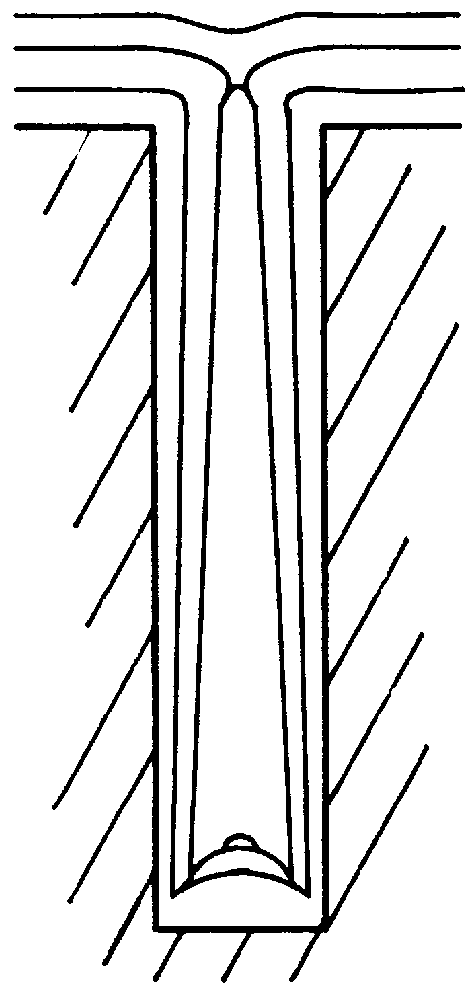
However, while either a THCVD or PECVD PSG or BPSG may be used to fill low aspect ratio (e.g. less than 1:1) features without voids, at higher aspect ratios the
gap filling capabilities of PECVD and THCVD processes diverge dramatically due to fundamental differences in the natures of these processes.
Thus step coverage in PECVD is usually poor and closure is usually observed at the tops of gaps requiring filling while voids are left lower in the gaps.
Furthermore, while THCVD may be practiced from mTorr pressures to atmospheric pressures (760
Torr) and above, PECVD is usually limited to a regime below 20
Torr due to the difficulty in maintaining a plasma at greater pressures.
Therefore, results achievable with PECVD may not be achieved with THCVD and vice-versa.
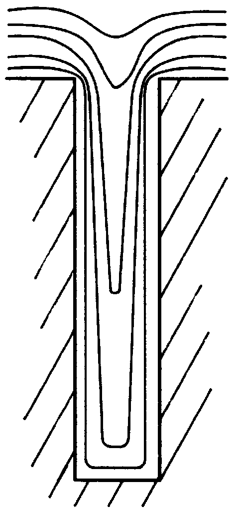
However, void-free
gap filling of the as deposited film is limited to aspect ratios of about 1:1.
All of these multi-step deposition and etch back processes use
reactive ion etching which subjects the substrate to potential device damage due to electrical charging.
This damage is detrimental to advanced logic and
DRAM devices where
gate oxide thicknesses may be as low as 50 Angstroms or less.
Furthermore, even with such multi-step processes, small voids are not reliably prevented.

