

Method of manufacturing semiconductor article
a manufacturing method and semiconductor technology, applied in the direction of semiconductor devices, basic electric elements, electrical appliances, etc., can solve the problems of limiting the freedom of device design, not being able to adapt to produce a large wafer, and expensive compound semiconductor substrates, etc., to achieve low power consumption of mosfets, reduce manufacturing costs, and reduce manufacturing costs
- Summary
- Abstract
- Description
- Claims
- Application Information
AI Technical Summary
Benefits of technology
Problems solved by technology
Method used
Image

Examples
example 1
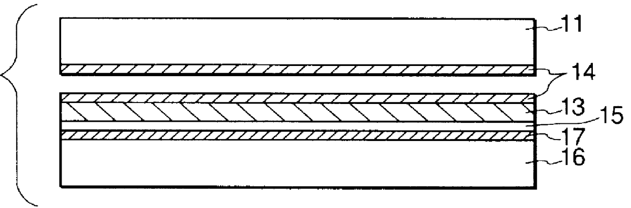
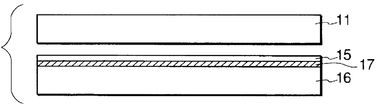
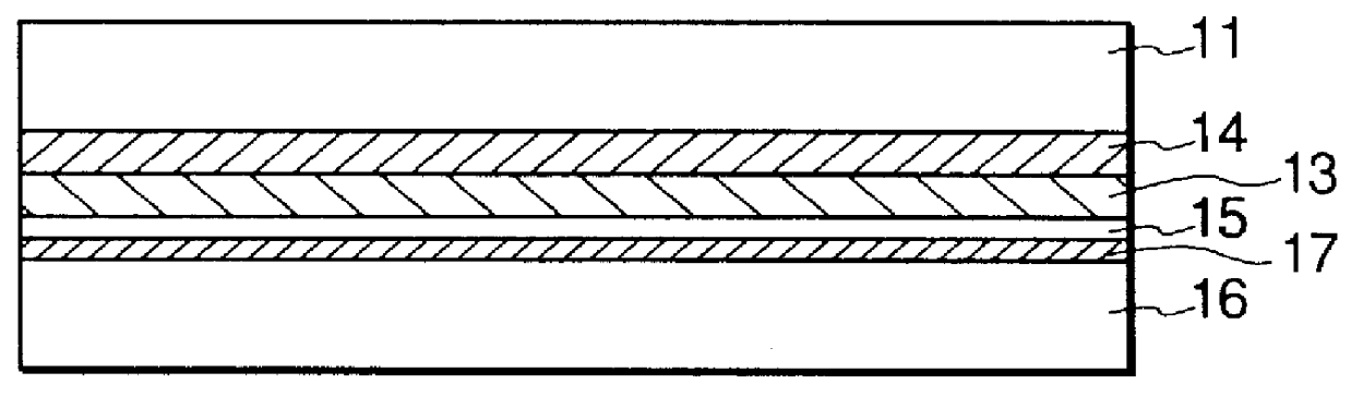
A 5 .mu.m thick P.sup.+ high concentration layer was formed as a surface layer of a single crystal silicon substrate having an unspecified electric resistance by means of a diffusion technique. Another P.sup.+ high concentration layer was also formed on the rear surface of the substrate.
More specifically, the P.sup.+ high concentration layer was formed in the following manner. A solution prepared by dissolving B.sub.2 O.sub.3 into a solvent was applied to the principal surface of an Si substrate by means of a spin-coating technique, which was then baked at 140.degree. C. to dissipate the solvent. The resultant substrate was then placed in a diffusion furnace and subjected to a so-called driven-in diffusion process to produce a P.sup.+ high concentration layer, maintaining the temperature of the furnace tube to 1,200.degree. C. for six hours. The spin-coated film was removed.
Subsequently, the Si substrate carrying thereon a P.sup.+ high concentration layer was immersed in an HF solut...
example 2
A 5 .mu.m thick P.sup.+ high concentration layer was formed as a surface layer of a single crystal silicon substrate having an unspecified electric resistance by means of a diffusion technique as in the case of Example 1. Another P.sup.+ high concentration layer was also formed on the rear surface of the substrate. The high concentration surface layer of the single crystal Si substrate was subjected to anodization in an HF solution. The anodization was conducted under the following conditions.
current density: 7 (mA.multidot.cm.sup.-2)
anodization solution: HF:H.sub.2 O:C.sub.2 H.sub.5 OH=1:1:1
duration: 11 (min.)
thickness of the porous Si layer: 12 (.mu.m)
The obtained porous silicon layer had a double-layered structure, of which the underlying lower porous silicon layer showed a minute and fragile structure if compared with the upper surface layer.
The substrate was then oxidized at 400.degree. C. for an hour in an oxygen atmosphere. As a result of the oxidation, the wall surfaces of t...
example 3
A 5 .mu.m thick P.sup.+ high concentration layer was formed as a surface layer of a single crystal silicon substrate having an unspecified electric resistance by means of a diffusion technique. Another P.sup.+ high concentration layer was also formed on the rear surface of the substrate.
More specifically, the P.sup.+ high concentration layer was formed by means of a diffusion technique in the following manner. An Si substrate was placed in a diffusion furnace and then N.sub.2 gas was introduced into a liquid diffusion source containing BBr.sub.3 for bubbling. The produced gas was then introduced into the furnace tube with a mixture carrier gas of (N.sub.2 +O.sub.2). A B.sub.2 O.sub.3 layer was formed by maintaining the temperature of the furnace tube to 1,050.degree. C. for an hour and subsequently the substrate was subjected to a so-called driven-in diffusion process to produce a P.sup.+ high concentration layer, maintaining the temperature of the furnace tube to 1,200.degree. C. f...
PUM
| Property | Measurement | Unit |
|---|---|---|
| thickness | aaaaa | aaaaa |
| thickness | aaaaa | aaaaa |
| thickness | aaaaa | aaaaa |
Abstract
Description
Claims
Application Information