It is therefore an object of the present invention to provide an apparatus for forming a silicon oxide film and a method of forming a silicon oxide film, in which a
metal portion of the apparatus is not corroded with water, and which are free from the problem of in-plane non-uniformity of the silicon oxide film caused by stains similar to water marks on the surface of the silicon semiconductor substrate.
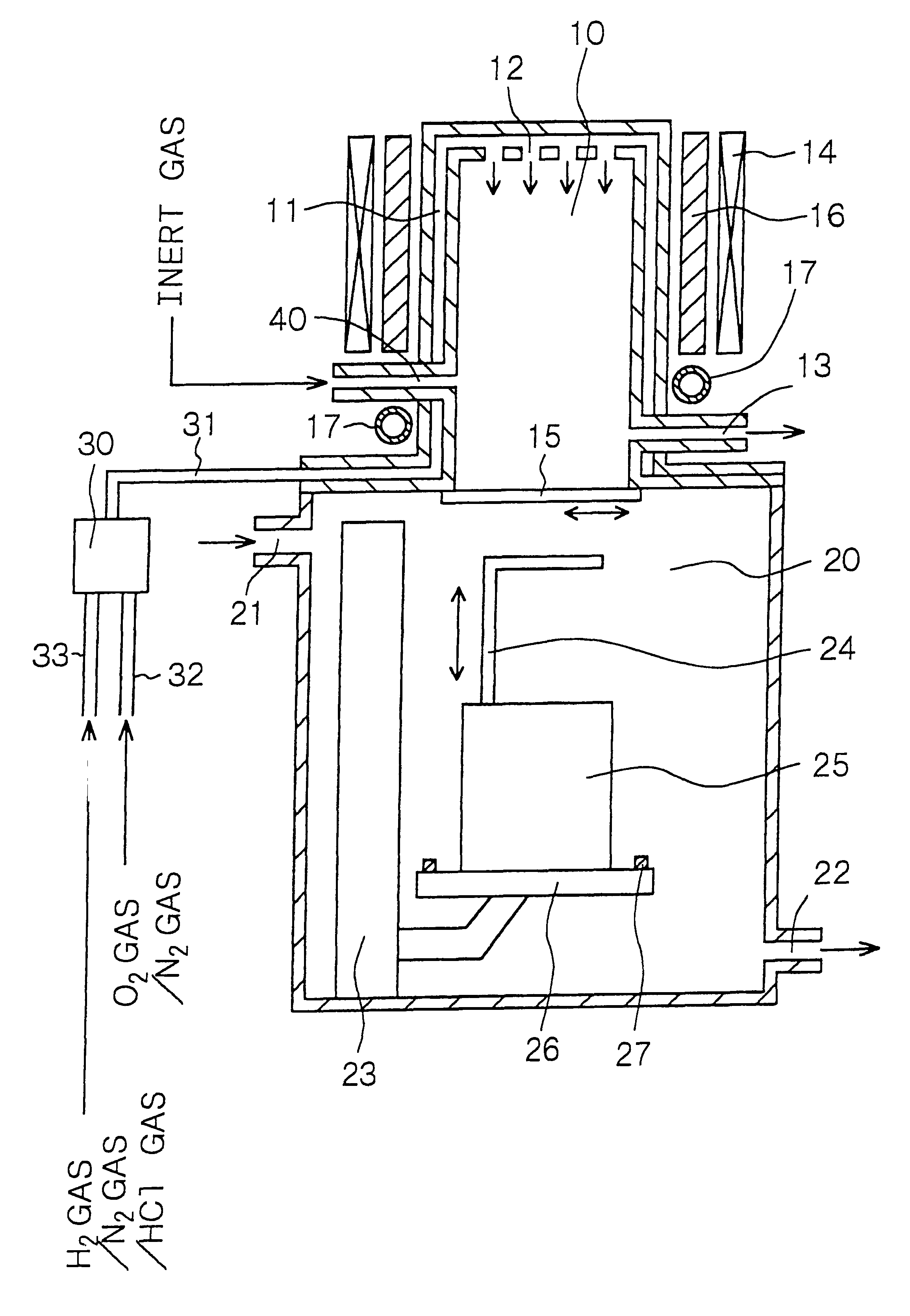
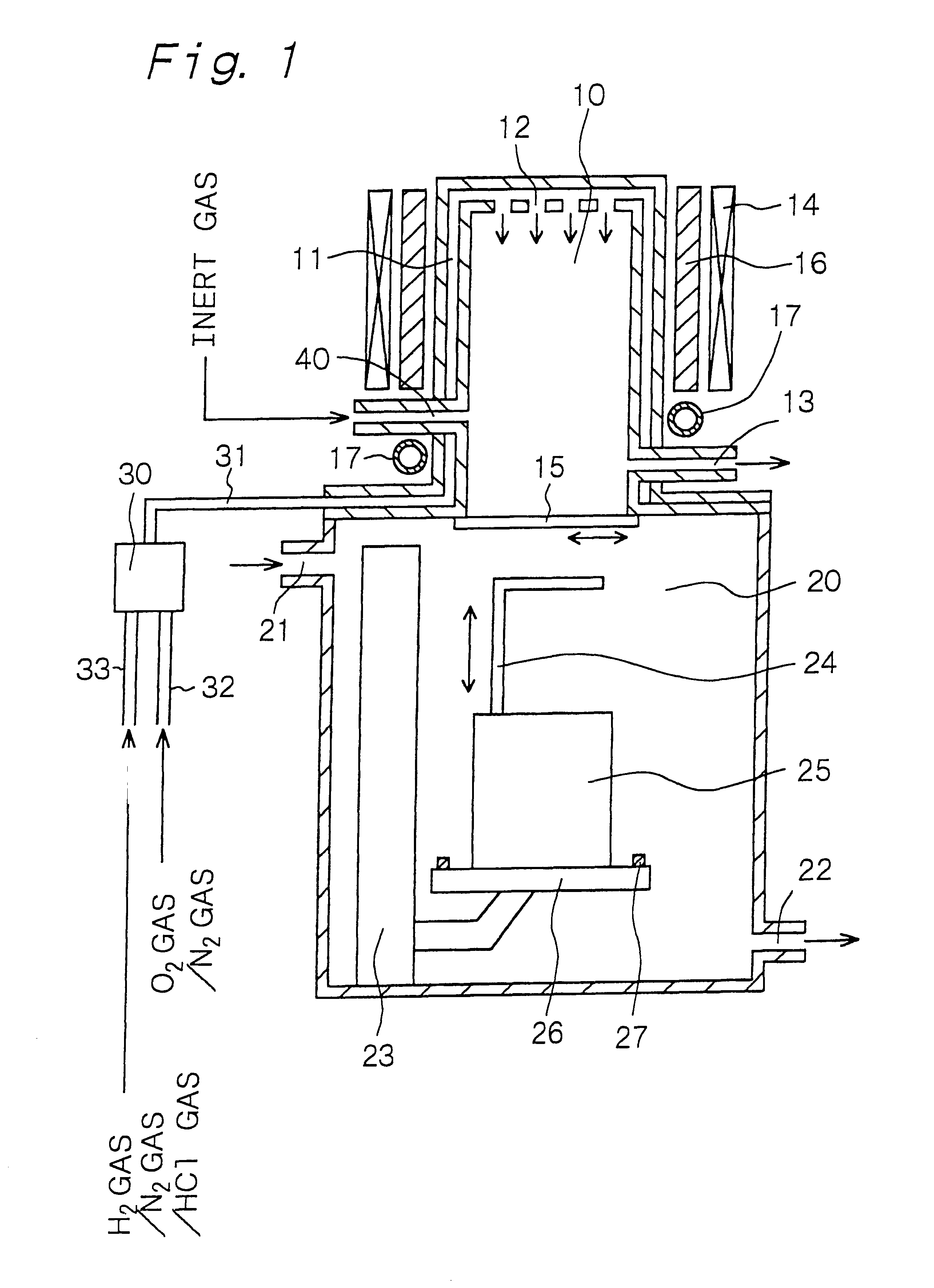
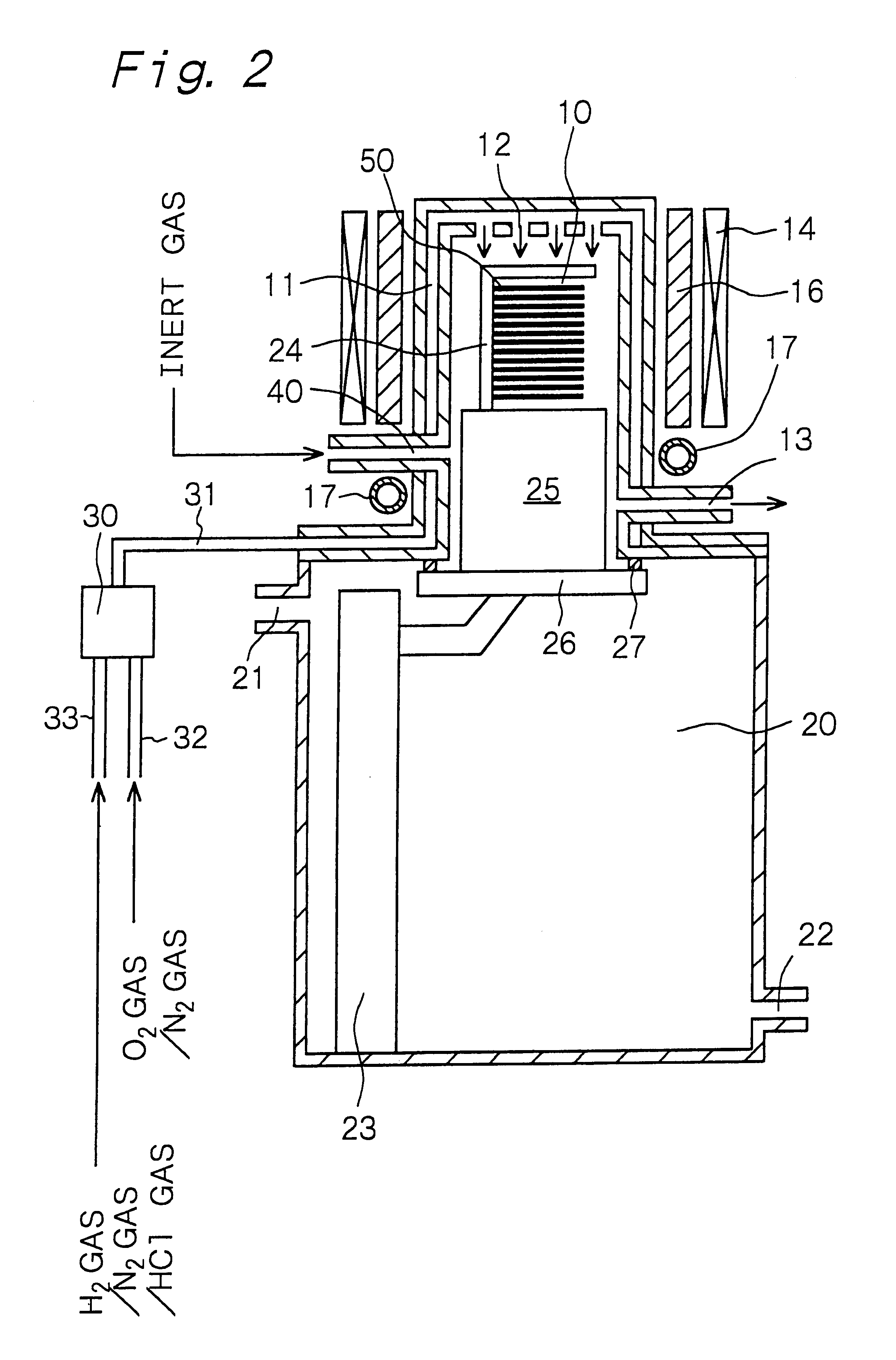
The apparatus for forming a silicon oxide film, provided by the present invention for achieving the above object, is an apparatus which has a process chamber and is for thermally oxidizing a surface of a silicon layer by introducing
water vapor into the process chamber, and which further has dew-formation prevention /
evaporation means for preventing dew formation in the process chamber and / or evaporating dew in the process chamber.
In the method of forming a silicon oxide film according to the second aspect of the present invention, preferably, the
inert gas exhausted out of the process chamber is measured for a
moisture content when the water vapor and / or dew are removed out of the process chamber, and after the
inert gas exhausted out of the process chamber has a
moisture content equal to, or smaller than, a predetermined value, the substrate is transferred out of the process chamber. The above predetermined value can be a value at which dew is not formed on a transfer unit such as the
elevator unit and the like when the substrate is transferred out with the transfer unit. That is, it can be a value equal to, or smaller than, a
saturated water vapor pressure in
atmosphere outside the process chamber. For example, preferably, it is 0.02 kg per
kilogram of dry
inert gas, while the predetermined value shall not be limited thereto. Further, preferably, the ambient temperature of the process chamber when the surface of the silicon layer is thermally oxidized and the ambient temperature of the process chamber when the water vapor and / or dew are removed out of the process chamber are nearly equal to each other, and in this case, the ambient temperature of the process chamber for the
thermal oxidation of the surface of the silicon layer is preferably 750.degree. C. or lower. The above "nearly equal" implies not only that the above two ambient temperatures are exactly the same but also that the above two ambient temperatures may be different to some extent (for example, by about 20.degree. C.). Hereinafter, "nearly equal" will imply as explained above. When the ambient temperature of the process chamber for and during the
thermal oxidation of the surface of the silicon layer is set at a value as explained above, a demand for a decrease in the thickness of the silicon oxide film can be satisfied, and
thermal shock on the substrates can be decreased.
In the method of forming a silicon oxide film according to the first aspect of the present invention, when the heat treatment is carried out in the process chamber subsequently to the
thermal oxidation, desirably, the ambient temperature in the process chamber in the heat treatment is adjusted to 700 to 1200.degree. C., preferably to 700 to 1000.degree. C., more preferably to 700 to 950.degree. C. Or, the ambient temperature in the process chamber in the heat treatment is preferably adjusted so as to be nearly equal to the ambient temperature for the thermal oxidation of the surface of the silicon layer in the process chamber. In the method of forming a silicon oxide film according to the second aspect of the present invention, when the heat treatment is carried out in the process chamber subsequently to the thermal oxidation, the ambient temperature for the heat treatment in the process chamber is preferably adjusted so as to be nearly equal to the ambient temperature for the thermal oxidation of the surface of the silicon layer in the process chamber. In these cases, the time period for the heat treatment is 5 to 60 minutes, preferably 10 to 40 minutes, more preferably 20 to 30 minutes. Since the heat treatment is carried out in a state where no dew is formed in the process chamber, after dew in the process chamber is evaporated, or after water vapor and dew in the process chamber are removed, the formation of, for example,
hydrochloric acid by a reaction of
hydrogen chloride and water can be reliably prevented when the heat treatment is initiated.
Before the silicon oxide film is formed on the silicon layer, generally, the surface of the silicon layer is cleaned by RCA cleaning in which the surface of the silicon layer is cleaned with an NH.sub.4 OH / H.sub.2 O.sub.2
aqueous solution and further cleaned with an HCl / H.sub.2 O.sub.2
aqueous solution, to remove fine particles and
metal impurities from its surface, and then the silicon layer is immersed in a
hydrofluoric acid aqueous solution. However, if the silicon layer is then exposed to
atmosphere, the surface of the silicon layer is contaminated, water or an organic substance may adhere to the surface of the silicon layer, or Si atoms in the surface of the silicon layer may bond to hydroxyl groups (OH) (for example, see "Highly-reliable
Gate Oxide Formation for
Giga-Scale LSIs by using Closed
Wet Cleaning System and
Wet Oxidation with Ultra-Dry Unloading", J. Yugami, et al., International
Electron Device Meeting Technical Digest 95, pages 855-858). In the above case, if the formation of the silicon oxide film is initiated in the above state, a resulting silicon oxide film includes water and an organic substance or Si--OH, which may
downgrade the characteristics of the silicon oxide film or may cause a defective portion. The defective portion refers to a portion of a silicon oxide film containing a silicon-
dangling bond (Si) or Si--H bond, or a portion of a silicon oxide film containing Si--O--Si bond which is compressed due to a stress or has a bond angle different from that of Si--O--Si in a thick or bulk silicon oxide film. For avoiding the above problem, therefore, it is preferred to include the step of cleaning the surface of the silicon layer before the formation of the silicon oxide film and carry out the step of forming the silicon oxide film without exposing the cleaned silicon layer to
atmosphere (for example, by maintaining an
inert gas atmosphere or a vacuum atmosphere in and from the cleaning of the surface of the silicon layer to the
initiation of formation of the silicon oxide film). In this manner, there can be formed the silicon oxide film on that surface of the silicon layer which is terminated with
hydrogen in most parts and terminated with
fluorine in vary small remaining parts, and the downgrading of characteristics of the formed silicon oxide film or the occurrence of defective portions can be prevented.
In the apparatus for forming a silicon oxide film or the method of forming a silicon oxide film according to the first aspect of the present invention, the dew-formation prevention /
evaporation means is provided. In the method of forming a silicon oxide film according to the second aspect of the present invention, the substrates are transferred out of the process chamber after an
inert gas atmosphere is provided in the process chamber and after water vapor and / or dew in the process chamber are removed. Therefore,
metal members constituting the apparatus for forming a silicon oxide film are not corroded with water, and there can be prevented the problem that stains similar to water marks occur on a surface of a silicon layer and cause an in-plane non-uniformity in the thickness of the silicon oxide film. Particularly, when a silicon oxide film is formed at an ambient temperature at which silicon atoms are not dissociated from the surface of the silicon layer, the above problems are liable to occur, while the present invention can reliably prevent the occurrence of the above problems. Otherwise, when an
inert gas atmosphere containing
halogen atom is provided in the process chamber to heat-treat the formed silicon oxide film subsequently to the formation of the silicon oxide film in the process chamber, and if water remains in the process chamber, for example,
hydrochloric acid is formed and it corrodes metal members constituting an apparatus for forming a silicon oxide film. In the present invention, the above phenomenon can be reliably prevented.

