Organic electroluminescent device having a conjugated polymer and an inorganic insulative electron injecting and transporting layer

a technology of electroluminescent devices and conjugated polymers, which is applied in the direction of discharge tubes/lamp details, discharge tubes luminescnet screens, other domestic articles, etc., can solve the problems of significant acceleration of the degradation of organic thin films, sensitivity to electrodes, and the formation of organic layers of organic materials

Inactive Publication Date: 2002-06-11
TDK CORPARATION
View PDF19 Cites 55 Cited by
  • Summary
  • Abstract
  • Description
  • Claims
  • Application Information

AI Technical Summary

Problems solved by technology

Reliability is a common problem to be solved for these organic EL devices.
However, the organic materials of which the organic layers are formed are vulnerable during manufacture and have less affinity to the electrodes.
Another problem is raised by the significantly accelerated degradation of organic thin films as compared with light emitting diodes (LED) and laser diodes (LD).
Although these devices are effectively and widely utilized, their size is so small that it is not only difficult, but also uneconomical to apply the LEDs to large area displays.
The ZnS system, however, suffers from serious practical drawbacks including the lack of reliability.
On practical use, these organic materials have the problems that they lack reliability like ZnS, and joining layers of these materials to current-injecting electrode layers is difficult.
The technique of depositing organic materials through sublimation leaves the problem that the resulting layers are soft and likely to recrystallize.
The technique of building up properly modified aromatic compounds by Langmuir-Blodgett method invites deterioration of film quality, dilution of active material, and an increase of manufacturing cost.
This device has the inconveniences of increased power consumption and low luminescence.
However, the materials used in the double layer structure are organic materials having the above-mentioned inconveniences.
Therefore, such a structure fails to exert electroluminescence.
The development of electroluminescence is utterly undesirable in

Method used


Image

  • Organic electroluminescent device having a conjugated polymer and an inorganic insulative electron injecting and transporting layer
  • Organic electroluminescent device having a conjugated polymer and an inorganic insulative electron injecting and transporting layer
  • Organic electroluminescent device having a conjugated polymer and an inorganic insulative electron injecting and transporting layer

Examples


example 1

A substrate of (7059) glass by Corning Glass Works was scrubbed using a neutral detergent.

By RF magnetron sputtering from a target of ITO oxide, a hole injecting electrode layer of ITO having a thickness of 200 nm was formed on the substrate at a temperature of 250.degree. C.

After its ITO electrode-bearing surface was cleaned with UV / O.sub.3, the substrate was secured by a holder for spin coating.

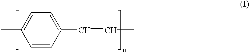
A methanol solution of a PPV precursor having a concentration of 1 g of polymer per 10 to 25 g of methanol was spin coated onto the substrate having the inorganic insulative hole injecting layer deposited thereon. This coating was carried out by applying the polymer solution to the entire surface of the substrate and then rotating the substrate at a revolution of up to 5,000 rpm while keeping its upper surface horizontal.

The substrate with the polymer precursor layer was heated for 12 hours in a vacuum oven at a temperature of 300.degree. C. This heat treatment converted the polymer precurs...

example 2

In Example 1, the main component, auxiliary component and stabilizer of the inorganic insulative electron injecting and transporting layer were changed from SrO to MgO, CaO or mixtures of these oxides, from Li.sub.2 O to K.sub.2 O, Rb.sub.2 O, K.sub.2 O, Na.sub.2 O, Cs.sub.2 O or mixtures of these oxides, and from SiO.sub.2 to GeO.sub.2 or oxide mixtures of SiO.sub.2 and GeO.sub.2, respectively, with substantially equivalent results. Similar results were obtained when the negative electrode forming material was changed from Al to Ag, In, Ti, Cu, Au, Mo, W, Pt, Pd, Ni or alloys thereof.

example 3

In Example 1, after its ITO electrode-bearing surface was cleaned with UV / O.sub.3, the substrate was secured by a holder in a vacuum evaporation chamber, which was evacuated to a vacuum of 1.times.10.sup.-4 Pa or lower.

Using a target of SiO.sub.2, an inorganic insulative hole injecting layer was deposited to a thickness of 2 nm. The sputtering gas used herein was a mixture of Ar and 5% of O.sub.2. Depositing conditions included a substrate temperature of 25.degree. C., a deposition rate of 1 nm / min, an operating pressure of 0.5 Pa, and an input power of 5 W / cm.sup.2. The hole injecting layer thus deposited had a composition of SiO.sub.1.9.

Thereafter, a PPV film was formed as in Example 1, and an inorganic electron injecting layer, an Al--Li (Li: 7 at %) film, and an Al film were formed, obtaining an organic EL device.

The resulting organic EL device was evaluated as in Example 1, finding substantially equivalent results.


PUM


Abstract

An organic electroluminescent device having high efficiency, a long life time, and low cost, includes a substrate, a hole injecting electrode and an electron injecting electrode formed on the substrate, an organic material-containing organic layer between the electrodes, and an inorganic insulative electron injecting and transporting layer between the light emitting layer and the electron injecting electrode. The organic layer includes a light emitting layer containing a conjugated polymer, and the inorganic insulative electron injecting and transporting layer comprises three components. The first component is at least one oxide selected from the group consisting of lithium oxide, rubidium oxide, potassium oxide, sodium oxide, and cesium oxide. The second component is at least one of strontium oxide, magnesium oxide, and calcium oxide. The third component consists of silicon oxide, germanium oxide, or mixtures thereof.

Description

Technical FieldThis invention relates to an organic electroluminescent (EL) device and more particularly, to an inorganic / organic junction structure suitable for use in a device of the type wherein an electric field is applied to a thin film of an organic compound to emit light.Background ArtActive research works have been made on organic EL devices for use as displays because EL devices can be formed on a large area of glass. In general, organic EL devices have a basic configuration including a glass substrate, a transparent electrode of tin-doped indium oxide (ITO) etc., a hole transporting layer of an organic amine compound, a light emitting layer of an organic fluorescent material exhibiting electronic conductivity and intense light emission such as an aluminum quinolinol complex (Alq3), and an electrode of a metal having a low work function such as MgAg, wherein the layers are stacked on the substrate in the described order.The device configurations which have been reported thu...

Claims


Application Information

Patent Timeline
IPC IPC(8): H01L51/50H01L51/52H05B33/12H05B33/22
CPCH01L51/5088H01L51/5092Y10S428/917H10K50/171H10K50/17H05B33/22
Inventor ARAI, MICHIOONITSUKA, OSAMU
Owner TDK CORPARATION
Why Eureka
Try Eureka