

Method for manufacturing polymer optical waveguide
- Summary
- Abstract
- Description
- Claims
- Application Information
AI Technical Summary
Benefits of technology
Problems solved by technology
Method used
Image

Examples
example 2
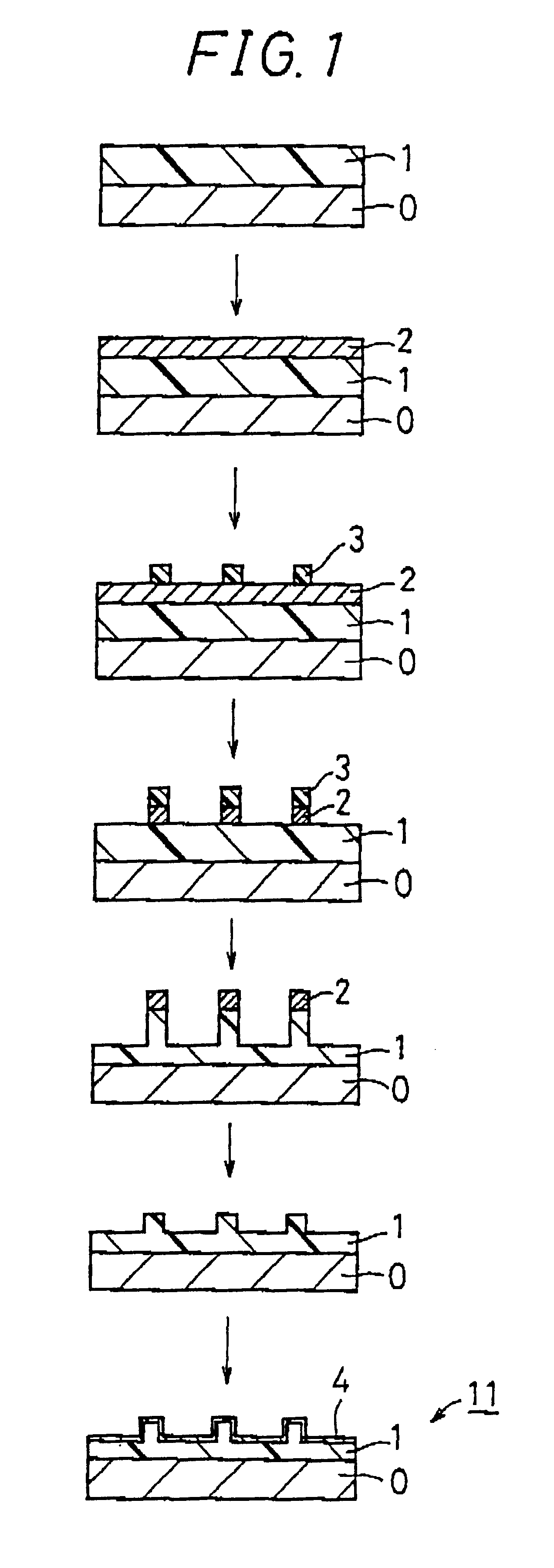
To a 4 inch-silicon substrate was applied 15 wt % N,N-dimethylacetamide (DMAc) solution of polyamide acids of 2,2-bis(3,4-dicarboxyphenyl)hexafluoropropane dianhydride (6FDA) and 2,2-bis(trifluoromethyl)-4,4'-diaminobiphenyl (TFDB) by the spin-coating method so that a film of 30 .mu.m thickness is formed after heating. A polyimide film was formed by subjecting it to heat treatment at 70.degree. C. for 2 hours, at 160.degree. C. for 1 hour, at 250.degree. C. for 30 minutes and at 350.degree. C. for 1 hour. A silicon-containing resist layer of 1.5 .mu.m thick is applied to the polyimide film, and thereafter pre-baked at about 90.degree. C. Then, after subjecting to the contact exposure using a photomask having a 40 line-linear optical waveguide pattern of 6 .mu.m width of line and 10 cm length at 100 .mu.m intervals, the photoresist on the exposed part was removed by development using a development solution. Then, post-bake was carried out at 90.degree. C. The polyimide film was etche...
example 3
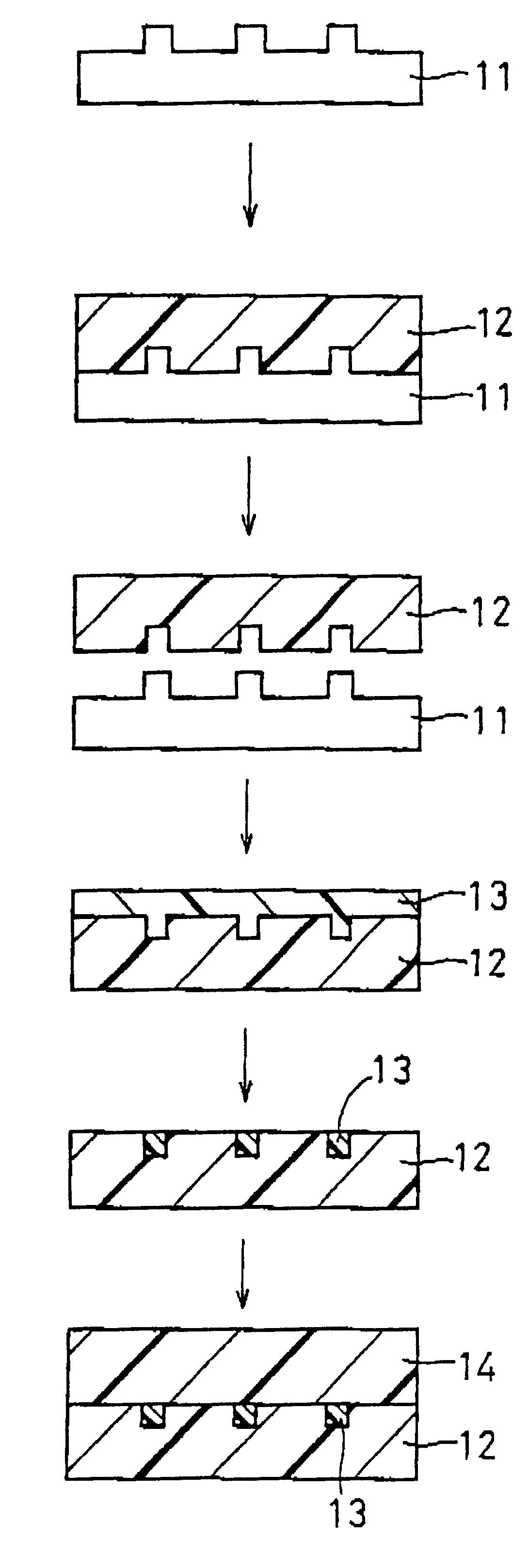
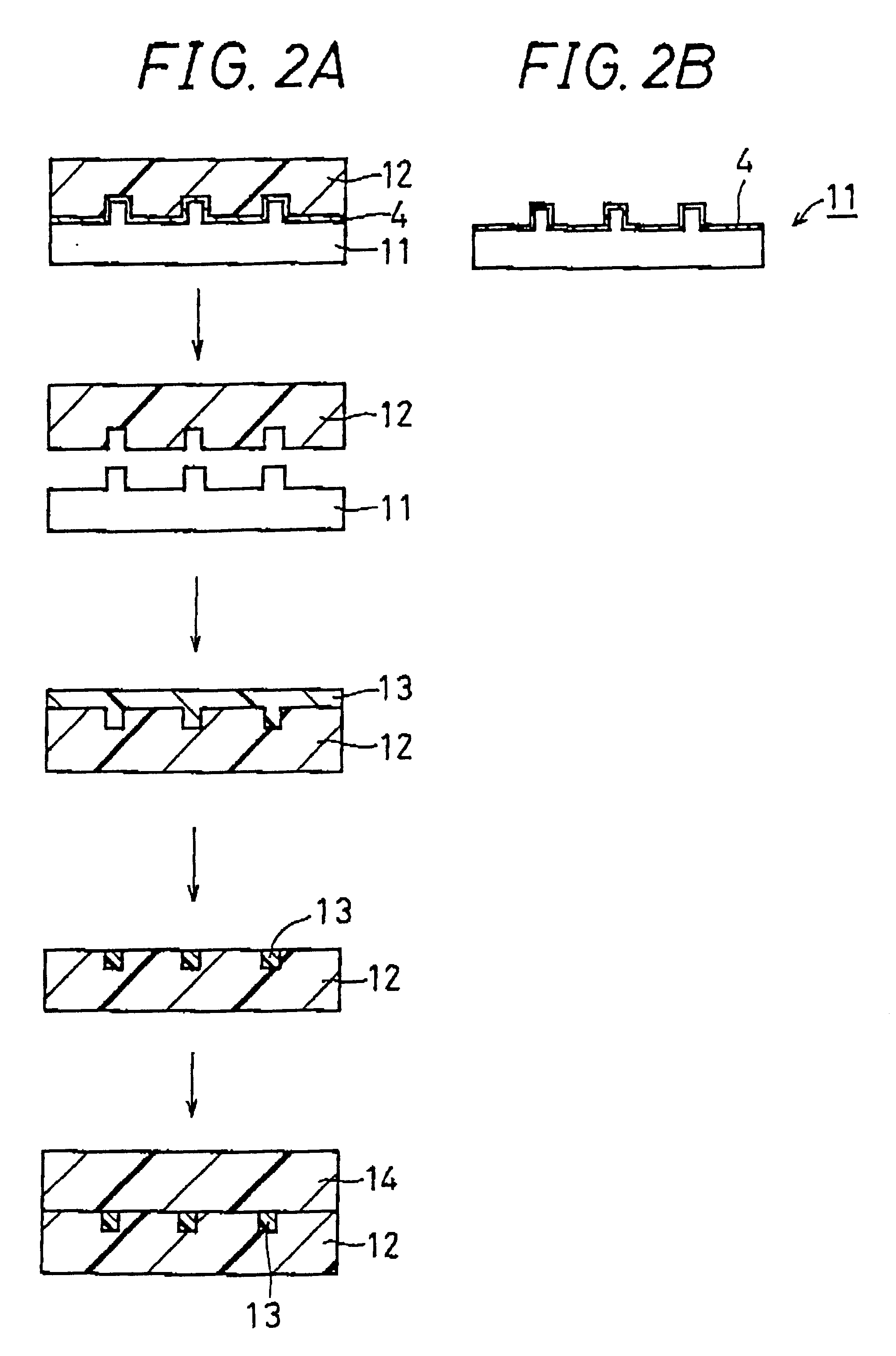
A mold for a polymer optical waveguide was manufactured by subjecting a 4 inch-wafer having a ridge of 6 .mu.m width and 6 .mu.m height formed by plasma etching to thermal oxidation so that a silicon oxide of 10 nm thickness was formed. Then, 15 wt % DMAc solution of polyamide acids of 6FDA and TFDB was coated on the mold by the printing method so that a film of 0.7 mm thickness is formed after heating. Thereafter, the polyimide film was stripped from the mold by soaking the mold and all in 2% aqueous hydrofluoric acid solution for etching silicon oxide, thereby forming a lower cladding layer. Then, a surface which had been contacted with the mold was turned upward, and by applying about 15 wt % DMAc solution of polyamide acids of 6FDA and 4,4'-oxydianiline (ODA) for forming the core layer on the surface of the lower cladding layer by spin-coating or the like and heating it for imide-formation, a core layer of polyimide was formed on the lower cladding layer. Then, an excess core la...
example 4
To a 4 inch-silicon substrate was applied 15 wt % N,N-dimethylacetamide (DMAc) solution of polyamide acids of 2,2-bis(3,4-dicarboxyphenyl)hexafluoropropane dianhydride (6FDA) and 2,2-bis(trifluoromethyl)-4,4'-diaminobiphenyl (TFDB) by the spin-coating method so that a film of 30 .mu.m thick is formed after heating. A polyimide film was formed by subjecting it to heat treatment at 70.degree. C. for 2 hours, at 160.degree. C. for 1 hour, at 250.degree. C. for 30 minutes and at 350.degree. C. for 1 hour. A silicon-containing resist layer of 1.5 .mu.m thickness was applied to the polyimide film, and thereafter pre-baked at about 90.degree. C. Then, after subjecting to the contact exposure using a photomask having a 40 line-linear optical waveguide pattern of 6 .mu.m width of line and 10 cm length at 100 .mu.m intervals, the photoresist on the exposed part was removed by development using a development solution. Then, post-bake was carried out at 90.degree. C. The polyimide film was etch...
PUM
| Property | Measurement | Unit |
|---|---|---|
| Thickness | aaaaa | aaaaa |
| Shape | aaaaa | aaaaa |
Abstract
Description
Claims
Application Information