Wiring material and a semiconductor device having wiring using the material, and the manufacturing method

a wiring material and semiconductor technology, applied in the direction of semiconductor devices, semiconductor/solid-state device details, instruments, etc., can solve the problems of operation error or deterioration of tft characteristics, and aluminum is not a preferred wiring material

Inactive Publication Date: 2003-09-02
SEMICON ENERGY LAB CO LTD
View PDF21 Cites 33 Cited by
  • Summary
  • Abstract
  • Description
  • Claims
  • Application Information

AI Technical Summary

Problems solved by technology

However, when a TFT is manufactured by using aluminum as a wiring material, operation error or deterioration of TFT characteristics were caused by formation of projections such as hillocks or whiskers or by dissemination of aluminum atoms into the channel forming region, in the heat treatment.
As stated above, aluminum is not a preferable wiri

Method used


Image

  • Wiring material and a semiconductor device having wiring using the material, and the manufacturing method
  • Wiring material and a semiconductor device having wiring using the material, and the manufacturing method
  • Wiring material and a semiconductor device having wiring using the material, and the manufacturing method

Examples


embodiments

Embodiment 1

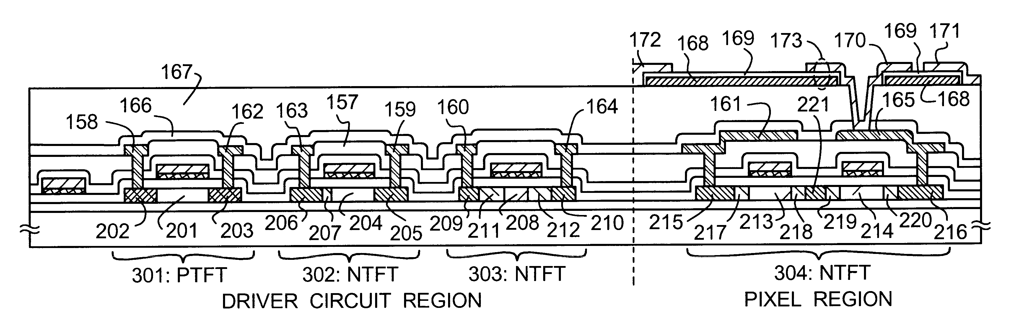
An embodiment of the present invention is explained by referring to FIGS. 1-5. Here, a manufacturing method for fabricating TFTs of pixel circuit and driver circuit disposed in the periphery at the same time is explained. Provided, for the simplicity of the explanation, CMOS circuits that are base circuits of shift register circuit, buffer circuit, etc., and n-channel TFT that forms sampling circuit are shown for the control circuit.

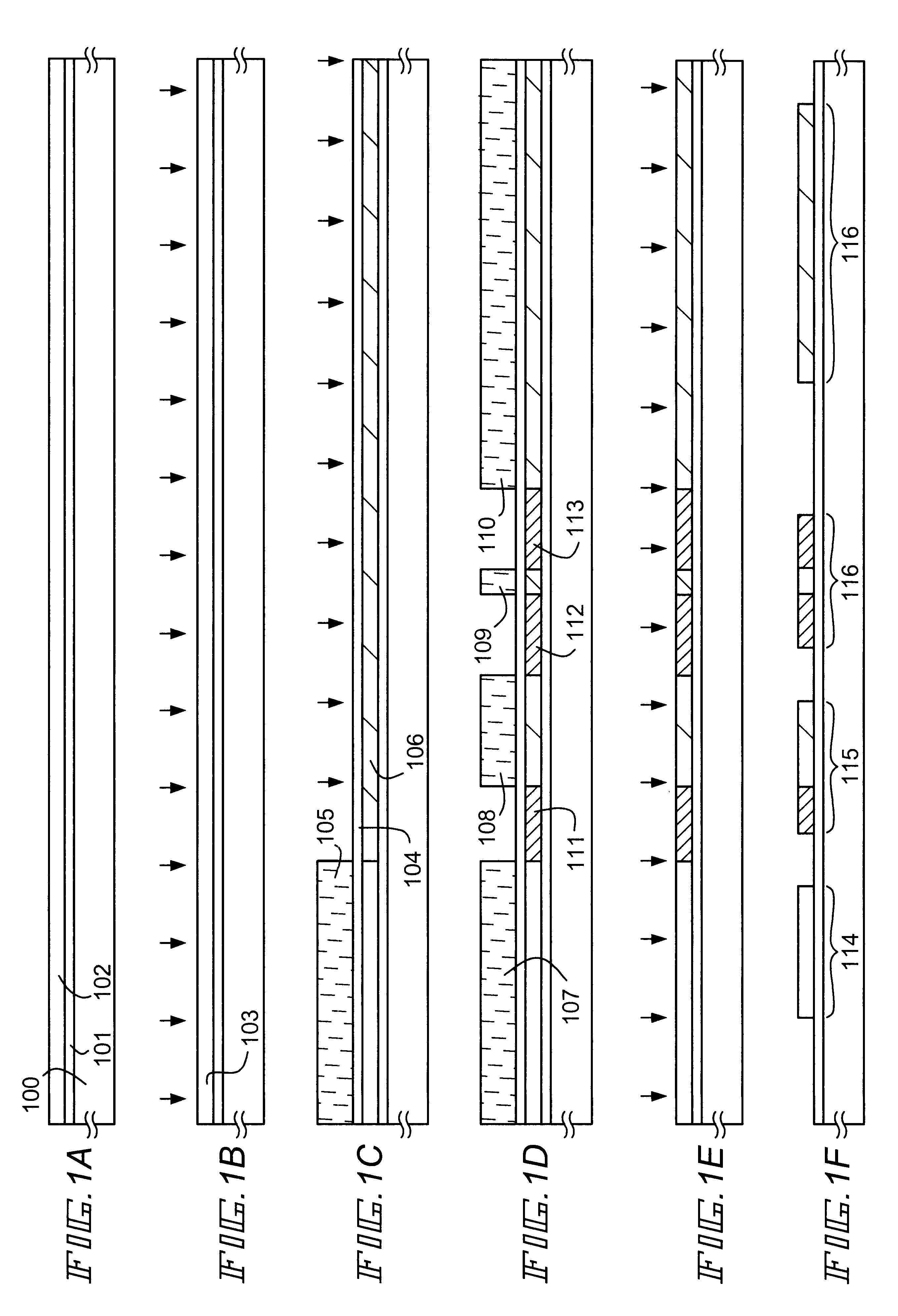
In FIG. 1(A), a glass substrate or a quartz substrate is preferably used as a substrate 100. A silicon substrate or a metal substrate having an insulating film on the surface thereof can be used, too. If heat resistivity permits plastic substrate may also be used.

A base film 101 that comprises a silicon-containing insulating film (the term "insulating film" generically represents a silicon oxide film, a silicon nitride film and a silicon nitride oxide film in this specification) is formed by plasma CVD or sputtering to a thickness of 100 to 4...

embodiment 3

[Embodiment 3]

A case of forming TFTs through different steps from those of embodiment 1 is described in embodiment 3 by using FIGS. 8A to 8D. Note that because only a part of the way is different from embodiment 1 and others are similar, same reference numerals are used for the same process. The example is given by the same impurity element as embodiment 1 for the impurity elements doped.

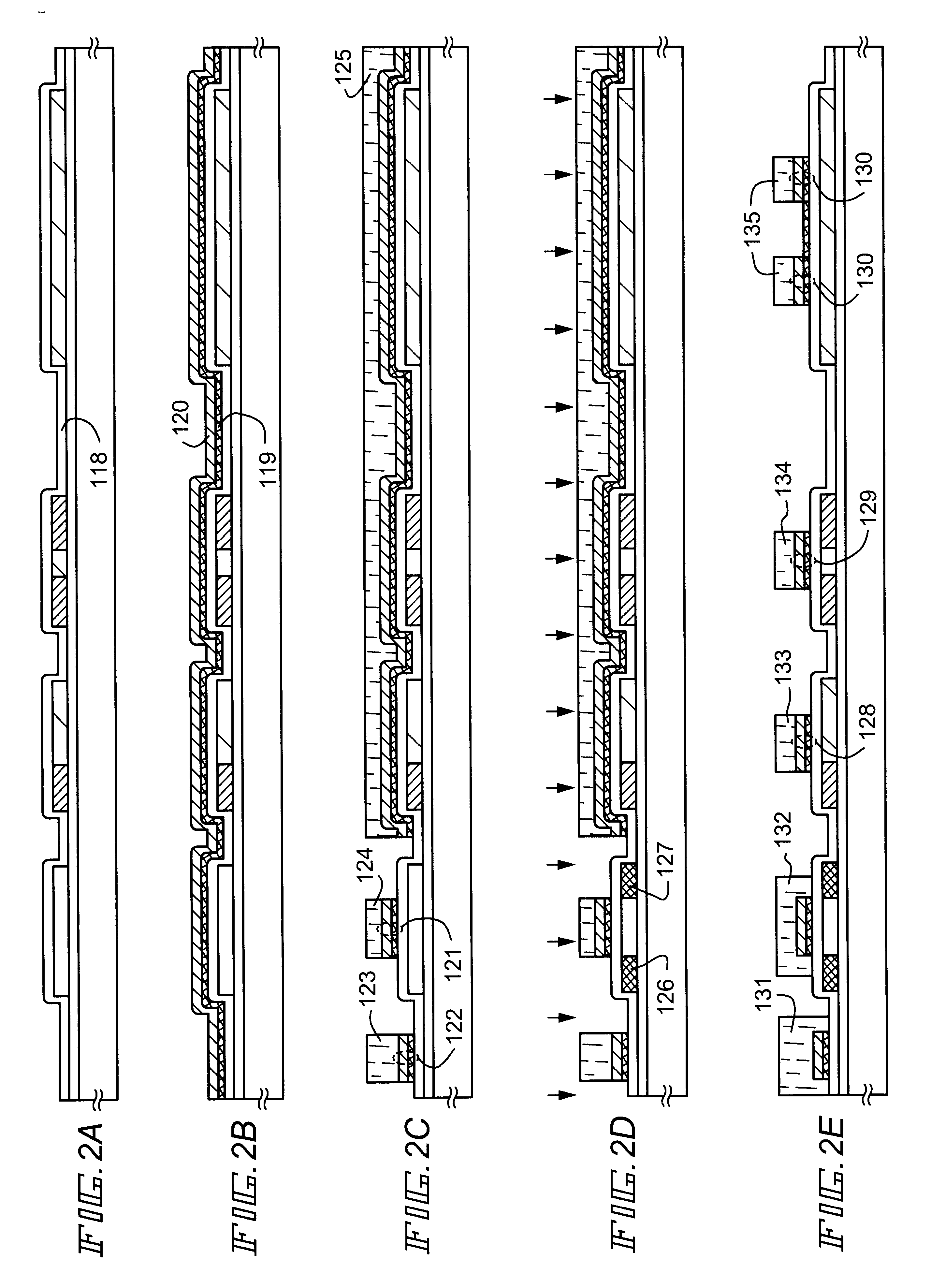
Firstly processes up to FIG. 3B are performed through the steps of embodiment 1. The figure corresponding to FIG. 3B is FIG. 8A.

After removing resist masks 131 to 135 and 140 to 142, nitrification process is performed onto gate wiring 121 and 128 to 130, and wiring 122.

The nitrification process here denotes a heat nitrification (heat treatment in an atmosphere containing ammonia or active nitrogen atoms) or plasma nitrification (a treatment in which plasma is generated by introducing ammonia gas or nitrogen gas into a reaction chamber under highly vacuum state and applying high frequency electric po...

embodiment 4

[Embodiment 4]

In embodiment 4 a case of manufacturing TFTs by a different process order from that of embodiment 1 is described. Note that only a part of the way is different from embodiment 1 and others are similar. The example is given by the same impurity element as embodiment 1 for the impurity elements doped.

First, up to a protection film 104 are formed by following the steps of embodiment 1. Resist masks are formed thereon to dope n-type impurity element under the same condition as FIG. 1D. Thus n-type impurity region (b) is formed.

The resist masks are removed next and new resist masks are formed. The channel doping process is performed under the same condition as FIG. 1C. Thus p-type impurity region (b) is formed.

From hereafter, processes from FIG. 1E may be performed according to embodiment 1. Note that it is possible to apply the structure of embodiment 4 in forming active matrix liquid crystal display device of embodiment 2.


PUM


Abstract

An object of the present invention is to realize a semiconductor device having a high TFT characteristic. In manufacturing an active matrix display device, electric resistivity of the electrode material is kept low by preventing penetration of oxygen ion into the electrode in doping of an impurity ion. A display device having a low electric resistivity can be obtained.

Description

1. Field of the InventionThe present invention relates to a semiconductor device having a circuit comprising a thin film transistor (hereinafter referred to as TFT). For example, the present invention relates to an electro-optical device, typically a liquid crystal display device, and an electronic device with an electro-optical device installed as a component.Note that through this specification, a semiconductor device indicates general devices that can function by using semiconductor characteristics, and that electro-optical devices, semiconductor circuits, and electronic devices are all categorized as semiconductor devices.2. Description of the Related ArtTechniques for using semiconductor thin films (with a thickness on the order of several nm to several hundreds of nm) formed on a substrate having an insulating surface to structure a thin film transistor (TFT) have been in the spotlight in recent years. Thin film transistors are widely applied to electronic devices such as ICs ...

Claims


Application Information

Patent Timeline
IPC IPC(8): H01L21/02H01L21/70H01L29/786H01L27/12H01L21/336H01L21/84H01L29/66G02F1/13G02F1/1362H01L21/77
CPCH01L29/4908H01L29/66757H01L29/78621H01L29/78624H01L29/78627H01L27/124G02F2001/13629G02F2001/136295H01L2924/0002H01L2924/00H01L2029/7863G02F1/13629G02F1/136295
Inventor YAMAZAKI, SHUNPEITAKAYAMA, TORU
Owner SEMICON ENERGY LAB CO LTD
Why Eureka
Try Eureka