Organic photovoltaic devices

a photovoltaic device and organic technology, applied in the direction of organic semiconductor devices, discharge tubes luminescnet screens, instruments, etc., can solve the problems of high cost and difficulty in production, poor stability of high efficiency amorphous silicon devices, and undesirable results of photosensitive optoelectronic devices, etc., to achieve the effect of great improvement efficiency

Inactive Publication Date: 2003-12-02
THE TRUSTEES FOR PRINCETON UNIV
View PDF16 Cites 455 Cited by
  • Summary
  • Abstract
  • Description
  • Claims
  • Application Information

AI Technical Summary

Benefits of technology

The present invention provides organic-based photosensitive optoelectronic devices with greatly improved efficiency. These devices comprise multiple stacked subcells in series between an anode layer and a cathode. Each subcell comprises an electron donor layer, and an electron acceptor layer in contact with the electron donor layer. The subcells are separated by an electron-hole recombination zone. Advantageously, the device also includes one or more exciton blocking layers (EBL) and a cathode smoothing layer.
A concentrator configuration can be employed to increase the efficiency of the device, where photons are forced to make multiple passes through the thin absorbing regions. Co-pending U.S. patent application Ser. No. 09 / 449,800 entitled "Highly Efficient Multiple Reflection Photosensitive Optoelectronic Device with Optical Concentrator" (hereinafter "'800 Application"), incorporated herein by reference, addresses this issue by using structural designs that enhance the photoconversion efficiency of photosensitive optoelectonic devices by optimizing the optical geometry for high absorption and for use with optical concentrators that increase collection efficiency. Such geometries for photosensitive devices substantially increase the optical path through the material by trapping the incident radiation within a reflective cavity or waveguiding structure, and thereby recycling light by multiple reflection through the thin film of photoconductive material. The geometries disclosed in the '800 Application therefore enhance the external quantum efficiency of the devices without causing substantial increase in bulk resistance. Included in the geometry of such devices is a first reflective layer; a transparent insulating layer which should be longer than the optical coherence length of the incident light in all dimensions to prevent optical microcavity interference effects; a transparent first electrode layer adjacent the transparent insulating layer; a photosensitive heterostructure adjacent the transparent electrode; and a second electrode which is also reflective.

Problems solved by technology

However, efficient crystalline-based devices, especially of large surface area, are difficult and expensive to produce due to the problems inherent in producing large crystals without significant efficiency-degrading defects.
On the other hand, high efficiency amorphous silicon devices still suffer from problems with stability.
Either of these outcomes is undesirable in a photosensitive optoelectronic device.
The result is that device configuration predictions from donor / acceptor criteria may not be borne out by actual device performance.
However, organic PV devices typically have relatively low quantum yield (the ratio of photons absorbed to carrier pairs generated, or electromagnetic radiation to electricity conversion efficiency), being on the order of 1% or less.
.), requiring a trade off between using a thick, and therefore resistive, cell with multiple or highly folded interfaces, or a thin cell with a low optical absorption efficiency.
Unfortunately, the obtained power conversion efficiency was less than for the single cell.
Therefore the photocurrent produced by the back cell is reduced, thus limiting the power conversion efficiency.
Additional reasoning was that doubling of the overall thickness in tandem devices results in increased series resistance, that also could affect the power conversion efficiency.

Method used


Image

  • Organic photovoltaic devices
  • Organic photovoltaic devices
  • Organic photovoltaic devices

Examples


Embodiment Construction

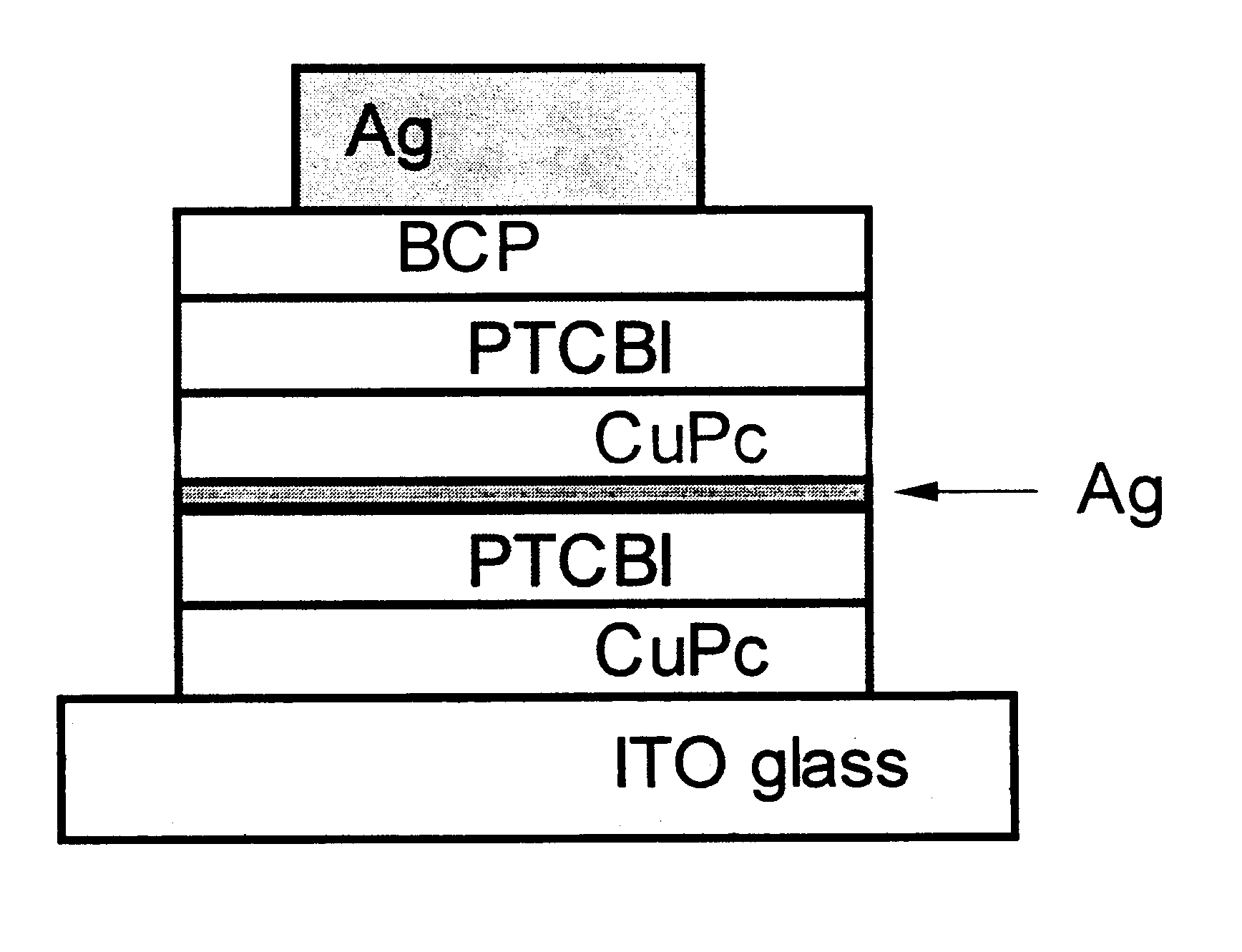
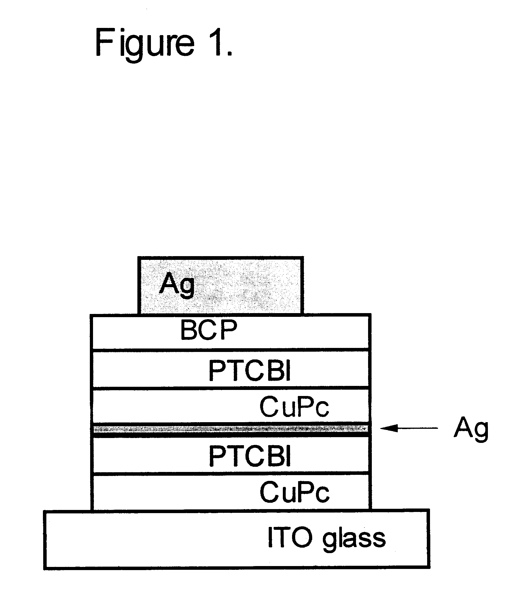
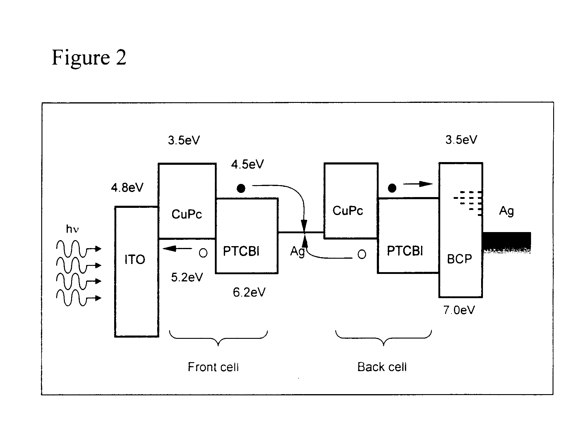
Exemplary embodiments are fabricated on pre-cleaned ITO glass substrates, spin-coated with a 300 .ANG. thick layer of polyethylenedioxythiophene:poystyrenesulfonate (PEDOT). Spin coating is performed at 4000 rpm for 40 sec, and is followed by 30 min drying at 110.degree. C. for 1 hour at reduced pressure. The organic materials are purified by train sublimation. The PV cells are formed by thermal evaporation (room temperature, 10.sup.-6 Torr, deposition rate of 1.5-2 .ANG. / sec) of organic materials on the ITO / PEDOT glass in the following sequence: donor-acceptor-metal-donor-acceptor-metal. The thickness of individual layers is controlled by use of, for example, a crystal oscillator thickness monitor. Copper phthalocyanine, CuPc, is used as a donor, and perylenetetracarboxylic bis-benzimidazole (PTCBI) as an acceptor. Ag is used for the thin (.about.5-20 .ANG.) layer between the front and the back cells and as a top metal electrode material. The top electrode (of 800 .ANG. thickness) ...


PUM

PropertyMeasurementUnit
thicknessaaaaaaaaaa
thicknessaaaaaaaaaa
thicknessaaaaaaaaaa

Abstract

The present invention generally relates to organic photosensitive optoelectronic devices. More specifically, it is directed to organic photovoltaic devices, e.g., organic solar cells. Further, it is directed to an optimized organic solar cell comprising multiple stacked subcells in series. High power conversion efficiency are achieved by fabrication of a photovoltaic cell comprising multiple stacked subcells with thickness optimization and employing an electron blocking layer.

Description

The present invention generally relates to organic photosensitive optoelectronic devices. More specifically, it is directed to organic photovoltaic devices, e.g., organic solar cells. Further, it is directed to an optimized organic solar cell comprising multiple stacked subcells in series.Optoelectronic devices rely on the optical and electronic properties of materials to either produce or detect electromagnetic radiation or to generate electricity from ambient electromagnetic radiation. Photosensitive optoelectronic devices convert electromagnetic radiation into electricity. Solar cells, also known as photovoltaic (PV) devices, are used to generate electrical power from ambient light. PV devices are used to drive power consuming loads to provide, for example, lighting, heating, or to operate electronic equipment such as computers or remote monitoring or communications equipment. These power generation applications often involve the charging of batteries or other energy storage devi...

Claims


Application Information

Patent Timeline
Patent Type & Authority Patents(United States)
IPC IPC(8): H01L27/28H01L27/30H01L31/0256H01L51/05H01L51/30B05D5/06H01L51/00H01L51/42
CPCH01L27/302H01L51/424H01L51/4246H01L51/0037H01L51/0053Y02E10/549H01L2251/308H01L51/0078H10K30/57H10K85/1135H10K85/621H10K85/311H10K30/20H10K30/211H10K2102/103
Inventor FORREST, STEPHEN R.YAKIMOV, AHARON
Owner THE TRUSTEES FOR PRINCETON UNIV
Why Eureka
Try Eureka