Protective hardmask for producing interconnect structures

a protective mask and interconnect technology, applied in the direction of semiconductor devices, semiconductor/solid-state device details, electrical apparatus, etc., can solve the problems of affecting the production efficiency of interconnect structures

Inactive Publication Date: 2004-04-13
IBM CORP
View PDF22 Cites 67 Cited by
  • Summary
  • Abstract
  • Description
  • Claims
  • Application Information

AI Technical Summary

Benefits of technology

The intermediate semiconductor device may further include a third hardmask layer disposed over the second hardmask layer, the third hardmask layer adapted to be removed during formation of interconnect structures in the semiconductor intermediate. Optionally, the intermediate semiconductor device may further include an etch stop layer disposed between the substrate and the bulk dielectric material and/or an embedded etch stop layer dividing the bulk dielectric material into upper and lower portions, the embedded etch stop layer adapted to provide uniform depth during subsequent etching of the bulk dielectric material.
In a fourth a...

Problems solved by technology

As semiconductor devices decrease in feature size, line-to-line capacitance becomes a problem.
However, during formation of the interconnects within the semiconductor device, even a desirably low k ILD is subject to processing conditions which may undesirably increase its dielectric constant thereby increasing the overall effective dielectric constant of the device as a whole.
During removal of excess metal used to form the int...

Method used


Image

  • Protective hardmask for producing interconnect structures
  • Protective hardmask for producing interconnect structures
  • Protective hardmask for producing interconnect structures

Examples


first embodiment

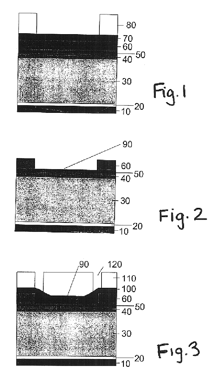
the present invention is depicted in FIGS. 1-10 comprising a dual damascene structure having a triple layer hardmask. A silicon semiconductor substrate 10 has deposited thereover an etch stop layer 20 comprising, for example, amorphous hydrogenated silicon carbide preferably that sold under the tradename BLoK.TM. by Applied Materials of Santa Clara, Calif. The thickness of etch stop layer 20 is preferably from about 10-100 nm, with a thickness of 50 nm being more preferred. Etch stop layer 20 ideally has the combined properties of not only being an etch stop layer but also a diffusion barrier to subsequent interconnect materials such as copper.

Etch stop layer 20 may also include such materials as silicon nitride, silicon carbide nitride, organo-silicate glass (OSG), silicon rich oxide (SiRO), silicon dioxide, organic siloxane polymer, carbon or hydrogen doped silicate glass or silsesquioxane glass, spin-on glass, fluorinated or non-fluorinated silicate glass, or any material know in...

third embodiment

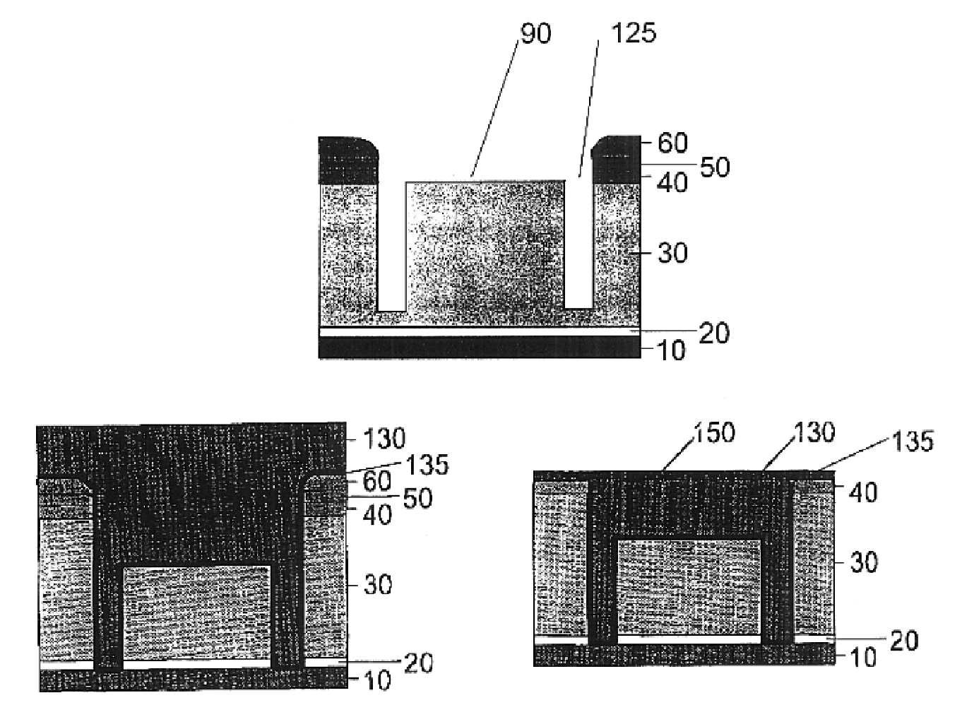
the present invention is depicted in FIG. 13 comprising a dual damascene structure having a bi-layer hardmask. The structure of FIG. 13 is similar to the structure of FIG. 1 except that the first low dielectric constant hardmask layer 40 is omitted. Fabrication proceeds in a manner similar to that described in connection with FIGS. 1-10 except that conditions for the CMP process are chosen such that hardmask layer 60 is removed while leaving hardmask layer 50 permanently in the structure. This structure has many advantages over structures known in the prior art and allows for the use of organic bulk low-k ILD 30 while providing tolerance for overlay errors, lithography rework capability, high performance, low cost and physical construction feasibility. In this embodiment the preferred bi-layer hardmask comprises PECVD silicon nitride with a thickness of about 35 nm (hardmask layer 50) and PECVD silicon dioxide layer with a thickness of about 150 nm (hardmask layer 60).

fourth embodiment

A fourth embodiment is depicted in FIG. 14 comprising a dual damascene structure having a bi-layer hardmask further including an embedded etch stop layer similar to the structure shown in FIGS. 1 and 13. As in FIG. 13, a low dielectric constant hardmask layer 40 is omitted. However, similar to FIG. 11, the bulk low-k ILD is comprised of two sections, a lower ILD 32 and an upper ILD 36 separated by embedded etch stop layer 34. Patterning proceeds identically to that discussed previously except that again hardmask layer 60 is removed while permanently retaining hardmask layer 50 in the final structure.

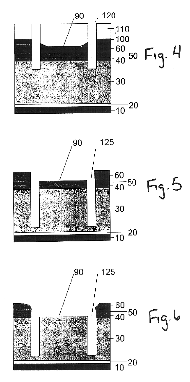
In a fifth embodiment comprising a single damascene structure with a triple layer hardmask, FIG. 15 illustrates a structure similar to the dual damascene structure of FIG. 1 except that bulk low-k ILD 30 now has a thickness of a desired line-level, and the etch stop layer 20 is optional. A photoresist layer 80 is patterned and etched, the pattern of which is etched into third hardmask la...


PUM


Abstract

The present invention provides a permanent protective hardmask which protects the dielectric properties of a main dielectric layer having a desirably low dielectric constant in a semiconductor device from undesirable increases in the dielectric constant, undesirable increases in current leakage, and low device yield from surface scratching during subsequent processing steps. The protective hardmask further includes a single layer or dual layer sacrificial hardmask particularly useful when interconnect structures such as via openings and/or lines are formed in the low dielectric material during the course of making the final product. The sacrificial hardmask layers and the permanent hardmask layer may be formed in a single step from a same precursor wherein process conditions are altered to provide films of differing dielectric constants. Most preferably, a dual damascene structure has a tri-layer hardmask comprising silicon carbide BLoK(TM), PECVD silicon nitride, and PECVD silicon dioxide, respectively, formed over a bulk low dielectric constant interlevel dielectric prior to forming the interconnect structures in the interlevel dielectric.

Description

1. Field of the InventionThis invention relates to a semiconductor device having an overall reduced dielectric constant and a method of producing the device utilizing a series of hardmask layers which protect an interlevel dielectric material of the device.2. Description of Related ArtAs semiconductor devices decrease in feature size, line-to-line capacitance becomes a problem. When metal lines of a semiconductor device are patterned closer and closer together, the dielectric constant k of any interlayer dielectric (ILD) material needs to be reduced in order to reduce the capacitive coupling between those lines. Thus, it is preferable to use an ILD having as low a dielectric constant as possible. However, during formation of the interconnects within the semiconductor device, even a desirably low k ILD is subject to processing conditions which may undesirably increase its dielectric constant thereby increasing the overall effective dielectric constant of the device as a whole. During...

Claims


Application Information

Patent Timeline
IPC IPC(8): H01L21/70H01L23/532H01L21/768H01L23/52H01L23/522H01L21/28H01L21/316H01L21/3205
CPCH01L21/76802H01L21/76811H01L21/76813H01L21/76816H01L21/76829H01L21/76835H01L23/5222H01L23/5329H01L2924/0002H01L2924/00H01L21/28
Inventor DALTON, TIMOTHY J.JAHNES, CHRISTOPHER V.LIU, JOYCE C.PURUSHOTHAMAN, SAMPATH
Owner IBM CORP
Why Eureka
Try Eureka