Damage-free sculptured coating deposition

a sculptured coating and sculpture technology, applied in the field of sculptured coating deposition, can solve the problems of difficult to use the techniques known in the art to provide multi-level metallurgy processing, the standard reactive ion etching method often used for patterning a blanket metal is particularly difficult with copper, and the applicability of alternative deposition lift-off techniques is limited

Inactive Publication Date: 2004-07-06
APPLIED MATERIALS INC
View PDF29 Cites 47 Cited by
  • Summary
  • Abstract
  • Description
  • Claims
  • Application Information

AI Technical Summary

Problems solved by technology

As the feature size of semiconductor patterned metal features has become increasingly smaller, it is particularly difficult to use the techniques known in the art to provide multilevel metallurgy processing.
The standard reactive ion etching method frequently used for patterning a blanket metal is particularly difficult with copper, since there are no volatile decomposition products of copper at low temperatures (less than about 200.degree. C.).
The alternative deposition lift-off techniques are also limited in applicability in a copper structure, given the susceptibility of copper to corrosion by the lift-off solvents.
Chemical vapor deposition, being completely conformal in nature, tends to create voids in the center of the filled opening, particularly in the instance of high aspect ratio features.
Further, contaminants from the deposition source are frequently found in the deposited conductive material, which may affect adhesion and other film properties.
Evaporation is successful in covering shallow features, but is generally not practical for the filling of high aspect ratio features, in part because the deposition rate for the evaporation technique is particularly slow, and also because of poor step coverage.
Electroplating has recently shown promise as a method of filling contact vias, but the crystal orientation of electroplated copper is not optimum for the reduction of electromigration unless a proper seed layer is deposited prior to electroplating.
Formation of such a continuous barrier layer is particularly difficult when the barrier layer must cover the surface of a feature having an aspect ratio of greater than about 3:1 and a feature size of 0.5 .mu.m or less.
The higher the ion energy, the more highly stressed the films, however.
However, Gamma sputtered TaN films exhibit a relatively high film residual compressive stress which can cause a Ta film or a tantalum nitride (e.g. Ta.sub.2 N or TaN) film to peel off from the underlying substrate (typically silicon oxide dielectric).
In the alternative, if the film does not peel off, the film stress can cause feature distortion on the substrate (typically a silicon wafer) surface or even deformation of a thin wafer.
The equipment required for collimated sputtering is generally difficult to maintain and difficult to control, since there is a constant build up of sputtered material on the collimator over time.
This overhang interferes with filling of the feature with a conductive material and may cause an increase in via / contact or line resistance.
Without sculpturing of the copper seed layer, there is typically too much overhang of deposited material at the top of a contact via.
This overhang leads to closure of the via opening prior to complete fill of the via, leaving voids inside the contact.
Absence of copper seed layer causes voids to form at the bottom of the via when due to lack of copper growth in that area.
(When the copper fill is deposited using electroplating, there is a lack of current for electroplating in areas where there is no copper seed layer.)
However, ion deposition sputtering can have adverse side effects in terms of erosion via sputtering of underlying layers which are contacted by the ion deposition sputtered material.
Further, the material eroded away from the underlying layer can contaminate adjacent surfaces of the feature.
Sputtering of the underlying substrate material can cause damage, destroy barrier layer properties, or poison a copper seed layer (e.g. low resistivity materials such as copper are extremely sensitive to impurities).

Method used


Image

  • Damage-free sculptured coating deposition
  • Damage-free sculptured coating deposition
  • Damage-free sculptured coating deposition

Examples


example two

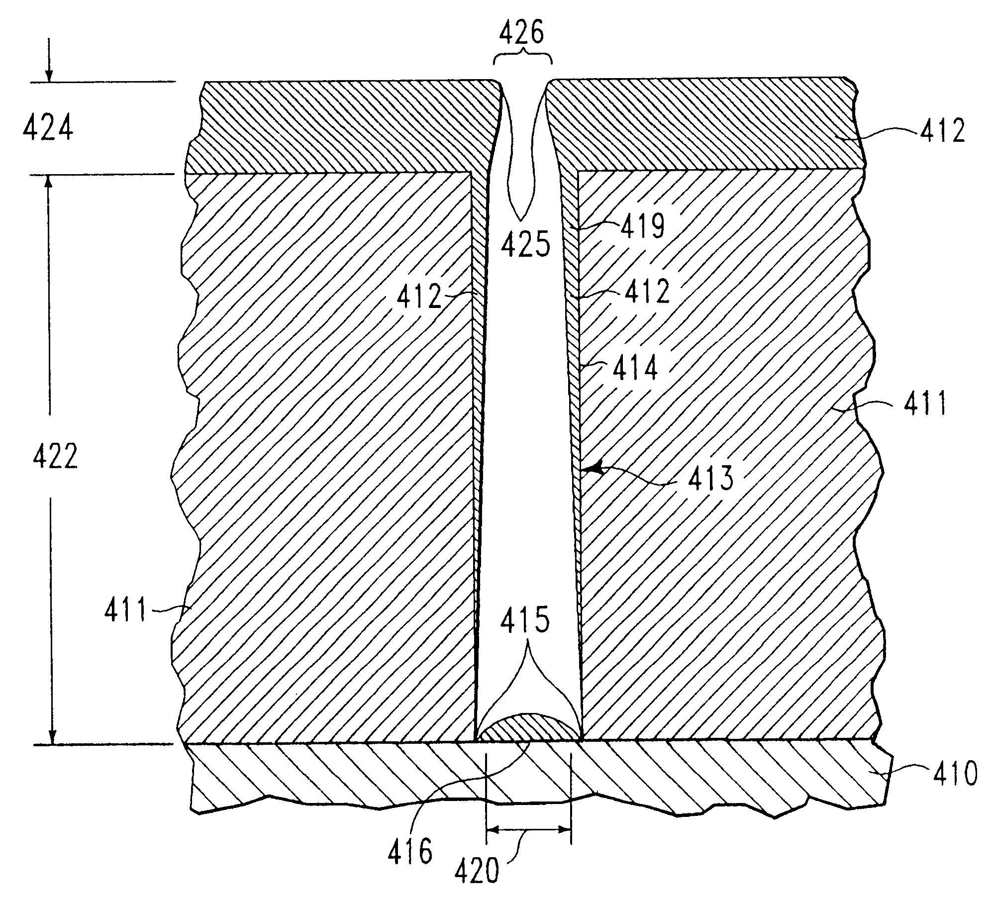
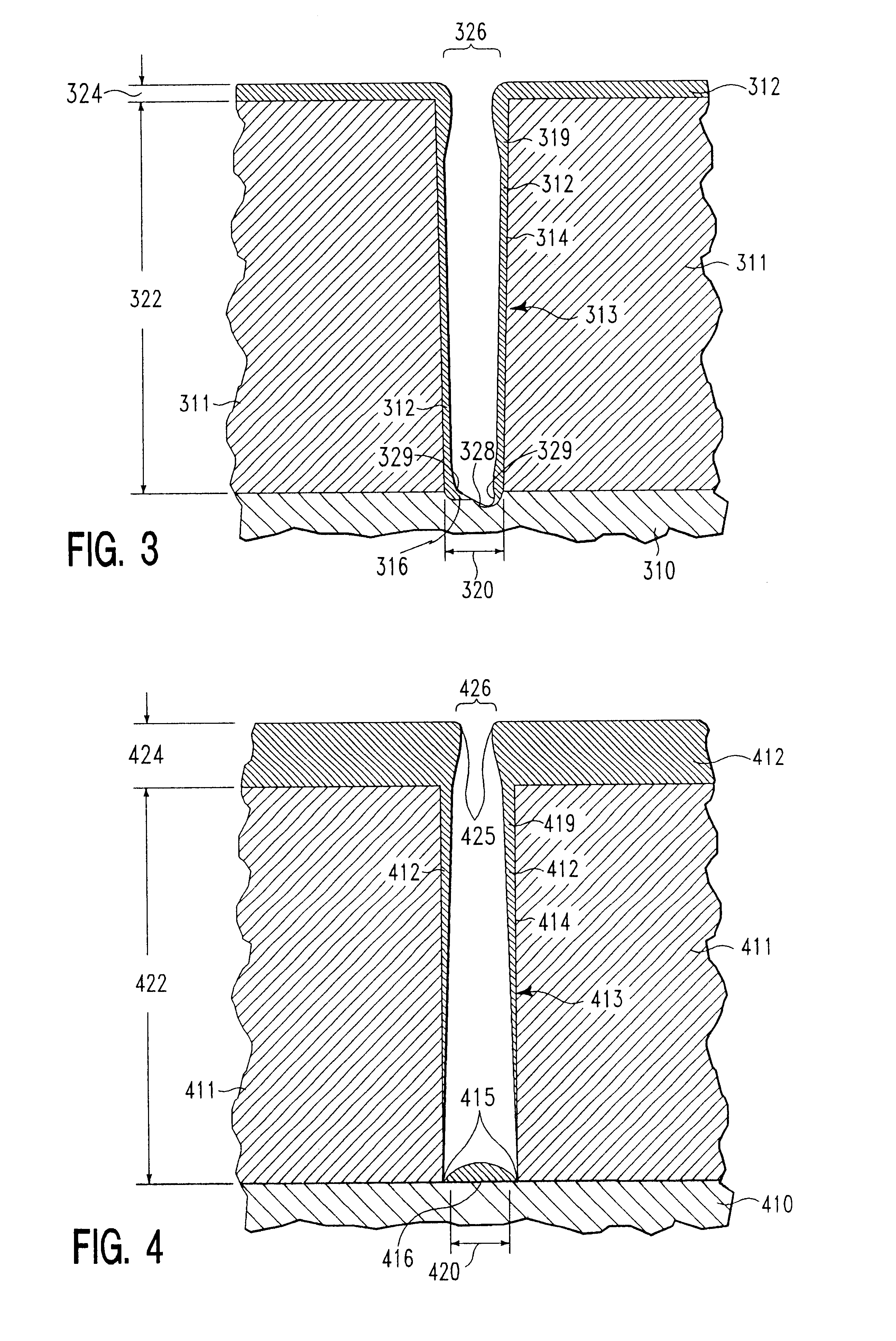
FIG. 4 shows a schematic of a SEM profile of a silicon wafer substrate 410 with a silicon dioxide dielectric layer 411 deposited thereover. The silicon dioxide layer 411 had been patterned to contain a via 413 having a bottom dimension 420 of 0.35 .mu.m and a height 422 of 1.2 .mu.m. A tantalum barrier layer 412 was applied over the surface 414 of the via 413 using an ion-deposition plasma process. In particular, the DC power to the target was 2 kW, the RF power to the coil (at 2 MHz) was 1.5 kW. In this instance there was no bias to the substrate. The pressure in the vacuum chamber was about 40 mT, and the temperature of the substrate at the time of deposition of the tantalum barrier layer 412 was about 75.degree. C. Tantalum was deposited for a period of about 60 seconds. The absence of substrate bias resulted in the deposit of a large quantity of tantalum at the bottom 416 of via 413. The tantalum layer 412 was about 1,200 .ANG. thick 424 on the substrate surface, about 400 .ANG....

example three

FIG. 5 shows a schematic of a SEM profile of silicon wafer substrate 510 with a silicon dioxide dielectric layer 511 deposited thereover. The silicon dioxide layer 511 had been patterned to contain a via 513 having a bottom dimension 520 of 0.35 .mu.m and a height 22 of 1.2 .mu.m. A tantalum barrier layer 512 was applied over the surface 514 of the via 513 using an ion-deposition plasma process. In particular, an initial deposition of tantalum was made using a DC power to the target was 2 kW, the RF power to the coil (at 2 MHz) was 1.5 kW, the pressure in the vacuum chamber was about 40 mT, and the substrate temperature was about 25.degree. C. Tantalum barrier layer 512 material was applied for about 15 seconds without the application of substrate biasing power.

The substrate bias was then applied to -60V (250 W), and additional tantalum was applied using ion deposition plasma for a period of about 45 seconds. The pressure in the vacuum chamber was about 40 mT and the substrate tempe...


PUM

PropertyMeasurementUnit
thicknessaaaaaaaaaa
sizeaaaaaaaaaa
aspect ratioaaaaaaaaaa

Abstract

We disclose a method of applying a sculptured layer of material on a semiconductor feature surface using ion deposition sputtering, wherein a surface onto which the sculptured layer is applied is protected to resist erosion and contamination by impacting ions of a depositing layer. A first protective layer of material is deposited on a substrate surface using traditional sputtering or ion deposition sputtering, in combination with sufficiently low substrate bias that a surface onto which the layer is applied is not eroded away or contaminated during deposition of the protective layer. Subsequently, a sculptured second layer of material is applied using ion deposition sputtering at an increased substrate bias, to sculpture a shape from a portion of the first protective layer of material and the second layer of depositing material. The method is particularly applicable to the sculpturing of barrier layers, wetting layers, and conductive layers upon semiconductor feature surfaces.

Description

1. Field of the InventionThe present invention pertains to a method of sputtering a sculptured coating over the walls of a high aspect ratio semiconductor feature in a manner which avoids or significantly reduces the possibility of damage to or contamination of underlying surfaces.2. Brief Description of the Background ArtAs the feature size of semiconductor patterned metal features has become increasingly smaller, it is particularly difficult to use the techniques known in the art to provide multilevel metallurgy processing. In addition, future technological requirements include a switch from the currently preferred metallurgy of aluminum to copper in some applications, because of copper's lower resistivity and higher electromigration resistance. The standard reactive ion etching method frequently used for patterning a blanket metal is particularly difficult with copper, since there are no volatile decomposition products of copper at low temperatures (less than about 200.degree. C....

Claims


Application Information

Patent Timeline
Patent Type & Authority Patents(United States)
IPC IPC(8): H01L21/70H01L21/768H01L21/285
CPCC23C14/046C23C14/165H01L21/2855H01L21/76843H01L21/76862H01L21/76865H01L21/76871H01L21/76877H01L21/76805H01L21/76844H01L21/76846H01L21/76879H01L21/76883
Inventor CHIANG, TONYYAO, GONGDADING, PEIJUNCHEN, FUSEN E.CHIN, BARRY L.KOHARA, GENE Y.XU, ZHENGZHANG, HONG
Owner APPLIED MATERIALS INC
Why Eureka
Try Eureka