
Fluorinated polythiophenes and devices thereof

a technology of fluorinated polythiophene and fluorinated polythiophene, which is applied in the field of polythiophene, can solve the problems of increased conductivity, increased conductivity, and reduced device performance, and achieves the effect of enhancing device performance and reducing manufacturing costs

Inactive Publication Date: 2005-02-15
XEROX CORP
View PDF10 Cites 26 Cited by
  • Summary
  • Abstract
  • Description
  • Claims
  • Application Information

AI Technical Summary

Benefits of technology

It is another feature of the present invention to provide certain poly(perfluoroalklylthiophene)s which are useful as microelectronic components, and which polythiophenes have reasonable solubility of, for example, at least about 0.1 percent by weight in common organic solvents, such as methylene chloride, tetrahydrofuran, toluene, xylene, mesitylene, chlorobenzene, and the like, and thus these components can be economically fabricated by solution processes such as spin coating, screen printing, stamp printing, dip coating, solution casting, jet printing, and the like.
Also, in yet another feature of the present invention there are provided poly(perfluoroalkylthiophene)s, and which polythiophenes are suitable for fabricating electronic device components under ambient conditions, thus enabling lower manufacturing cost.
Additionally, in a further feature of the present invention there is provided a class of poly(perfluoroalkylthiophene)s with unique structural features which are conducive to molecular self-alignment under appropriate processing conditions, and which structural features also enhance the stability of device performance.
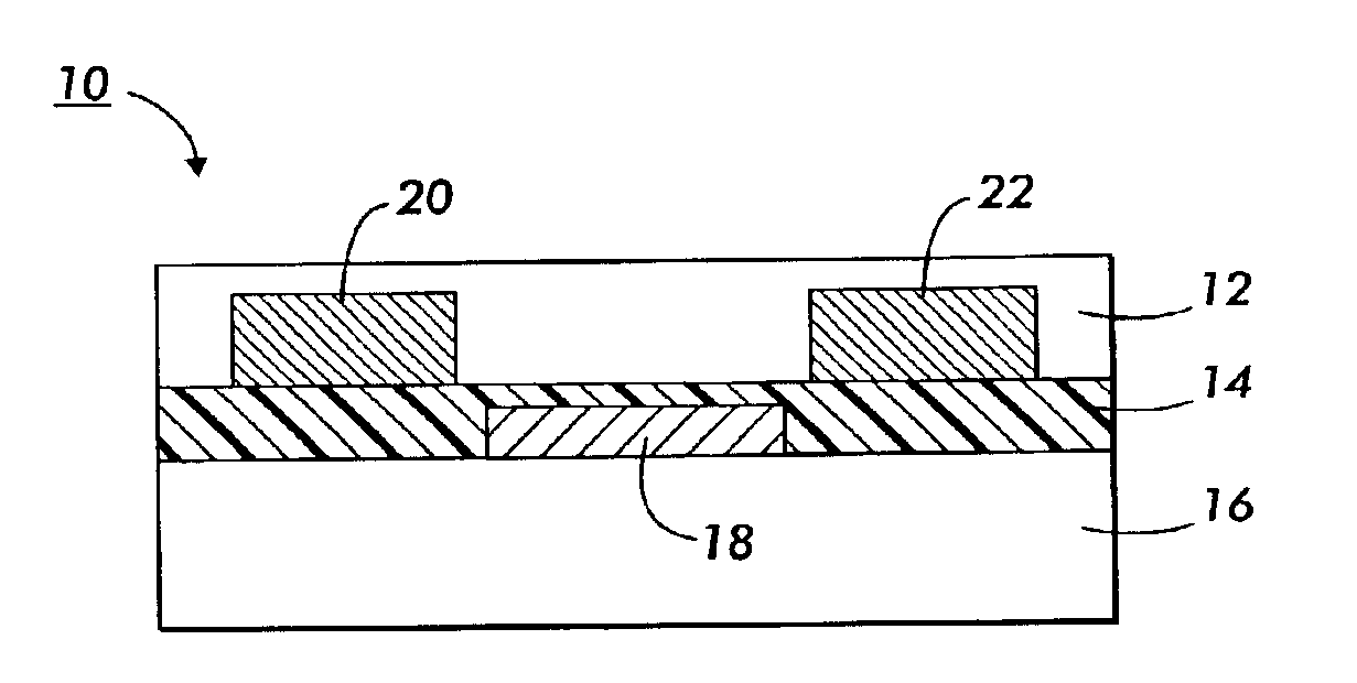
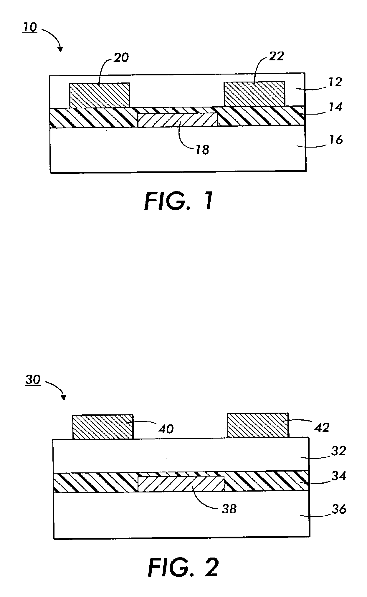
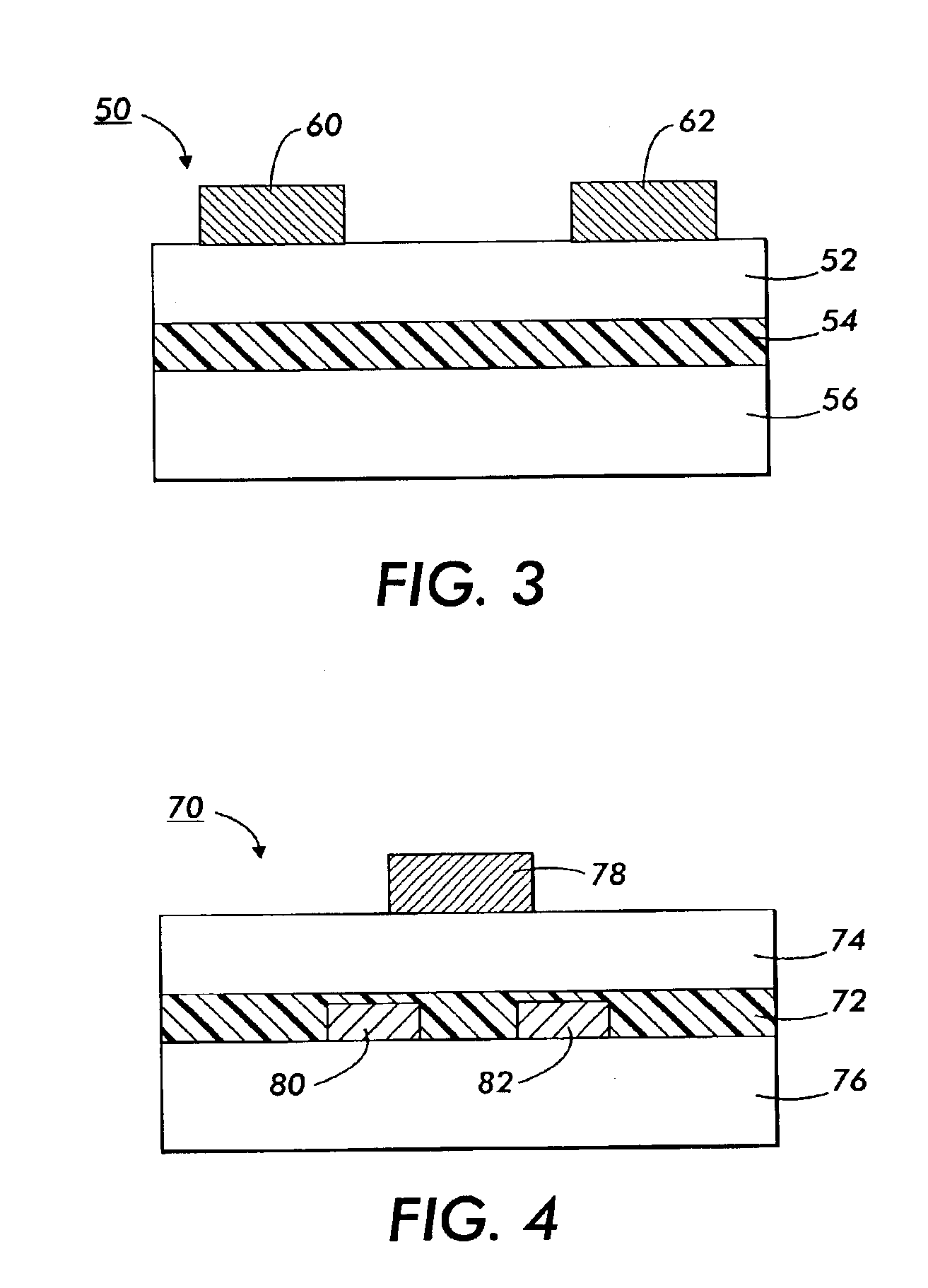
In embodiments the polythiophenes illustrated herein are soluble in common coating solvents, for example, in embodiments the polythiophenes possess a solubility of at least about 0.1 percent by weight, and more specifically, from about 0.5 percent to about 5 percent by weight in such solvents as methylene chloride, 1,2-dichloroethane, tetrahydrofuran, toluene, xylene, mesitylene, chlorobenzene, and the like. Moreover, the polythiophenes of the present invention in embodiments, when fabricated as semiconductor channel layers in TFT devices, provide a stable conductivity of, for example, from about 10−9 S / cm to about 10−6 S / cm, and more specifically, from about 10−8 S / cm to about 10−7 S / cm as determined by conventional four-probe conductivity measurements. Further, the polythiophenes possess side chains that are regioregularly positioned on the polythiophene backbone. These strategically positioned side chains of (I) facilitate proper alignment of side chains, enabling formation of higher-order microstructure domains in thin films. It is believed that these polythiophenes, when fabricated from solutions as thin films of, for example, about 10 nanometers to about 500 nanometers, form closely stacked lamella structures that are conducive to efficient charge carrier transport. The polythiophenes of the present invention in embodiments can enable formation of semiconductor layers using common deposition techniques, such as solution coating or jet printing in ambient conditions without costly precautionary measures in excluding ambient oxygen during device fabrication. Fabrication in ambient conditions is critical to low cost manufacturing.

Problems solved by technology

Fabrication by common solution processes could render the manufacturing of TFTs by a noncomplex cost effective manner in comparison to the costly conventional photolithographic processes typical of silicon-based devices such as hydrogenated amorphous silicon.
Nonetheless, a number of the semiconductor polythiophenes may not be suitable for fabrication in ambient environments since they tend to be oxidatively doped by atmospheric oxygen, resulting in increased conductivity, thus in larger off-current and lower current on / off ratio for the devices fabricated from these materials.
These precautionary measures add to the cost of manufacturing, therefore offsetting the appeal of certain polymer TFTs as an economical alternative to amorphous silicon technology, particularly for large area devices.

Method used


Image

  • Fluorinated polythiophenes and devices thereof
  • Fluorinated polythiophenes and devices thereof
  • Fluorinated polythiophenes and devices thereof

Examples


example i

Preparation of Polythiophene (1, a=0.75; b=0.25)

i) Monomers

2,5-Dibromo-3-hexylthiophene was prepared by adding 35.60 (0.20 mol) of powdered N-bromosuccinimide to 16.83 grams (0.10 mol) of 3-hexylthiophene in 135 milliliters of 1:1 mixture of dichloromethane and acetic acid at room temperature over a period of 30 minutes. The mixture was then stirred for about 4 hours at room temperature and the progress of the reaction was monitored by TLC. After the reaction, the reaction mixture was diluted with 100 milliliters of dichloromethane and transferred to separatory funnel. The organic phase was separated and washed three times with water, two times with a 10 percent aqueous sodium bicarbonate solution, 2 times with a 5 percent aqueous sodium thiosulfate solution, and then three times with water again. The organic layer was separated and dried with magnesium sulfate, and the solvent removed by vacuum evaporation. Pure, about 99.5 percent, 2,5-dibromo-3-hexylthiophene was obtained by dist...


PUM

PropertyMeasurementUnit
mole fractionsaaaaaaaaaa
conductiveaaaaaaaaaa
stabilityaaaaaaaaaa

Abstract

An electronic device containing a polythiophene wherein R is an alkyl alkoxy; x represents the number of R groups; R′ is CF3, alkoxy, alkyl, or optionally alkylene; y and z represent the number of segments; and a and b represent the mole fractions of each moiety, respectively, wherein the sum of a+b is equal to about 1.

Description

BACKGROUNDThe present invention is generally directed to polythiophenes and uses thereof. More specifically, the present invention in embodiments is directed to electronic devices, such as thin film transistors (TFT), containing a novel class of polythiophenes, especially poly(perfluoroalkylthiophenes) wherein certain repeating thienylene units possess perfluoroalkyl and alkyl side chains, which are arranged in a regioregular manner on the polythiophene backbone, and which polythiophenes are, for example, useful as active semiconductor materials in thin film transistors. In embodiments the polythiophenes, which can be comprised of, for example, two monomers such as 3-alkylthiophene and 3-perfluoroalkylthiophene in various effective proportions, possess the ability to self-organize when coated from their solutions into molecularly ordered thin films. The self-organization is a result, it is believed, of the intermolecular interaction between the side chains.The polythiophenes of the ...

Claims


Application Information

Patent Timeline
Patent Type & Authority Patents(United States)
IPC IPC(8): C08G61/00C08G61/12H01L51/30H01L51/05
CPCC08G61/126H01L51/0036H01L51/0545H01L51/0541H10K85/113H10K10/466H10K10/464
Inventor ONG, BENG S.JIANG, LUWU, YILIANGLIU, PING
Owner XEROX CORP
Learn More