Low firing temperature thick film dielectric layer for electroluminescent display

Inactive Publication Date: 2005-07-19
IFIRE IP CORP
View PDF5 Cites 14 Cited by
  • Summary
  • Abstract
  • Description
  • Claims
  • Application Information

AI Technical Summary

Benefits of technology

[0013]The present invention is a composite thick film dielectric layer that can be sintered onto a glass material substrate at temperatures below the softening temperature of the glass material substrate without significantly increasing the residual porosity of the t

Problems solved by technology

However, the dielectric breakdown strength of these dielectric materials is relatively low, necessitating the use of a relatively thick dielectric layer, typically greater than 10 micrometers, to prevent dielectric breakdown during display operation.
This makes it more difficult to smooth the surface of the thick film dielectric layer using a sol gel or MOD process, and tends to red

Method used


Image

  • Low firing temperature thick film dielectric layer for electroluminescent display
  • Low firing temperature thick film dielectric layer for electroluminescent display
  • Low firing temperature thick film dielectric layer for electroluminescent display

Examples


example 1

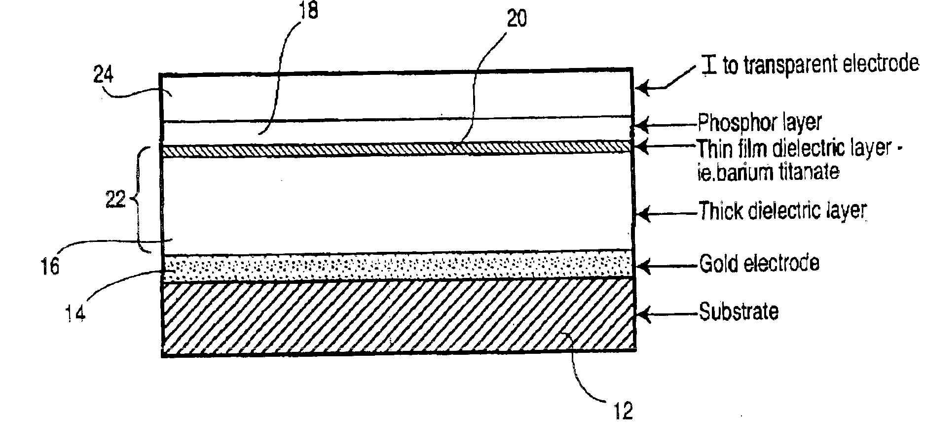
[0116]With reference to FIG. 1, an electroluminescent device was constructed on a 5 centimeter by 0.5 centimeter by 5 centimeter thick PP8C glass substrate obtained from Nippon Electric Glass Co. Ltd. Of Osaka, Japan using the general methods described in U.S. patent application Ser. No. 09 / 540,288 in combination with the methods described herein. The device had a barium titanate barrier layer between the thick dielectric layer as described in Applicant's co-pending U.S. patent application Ser. No. 09 / 761,971 filed Jan. 17, 2001 (the contents of which are incorporated herein by reference) and a 0.5 micron thick zinc sulfide phosphor layer. The lower electrode was gold and the upper transparent electrode was indium tin oxide (ITO).

[0117]The thick film dielectric paste was formulated with perovskite-forming powdered precursor materials including 600 grams of PMN obtained from Ferro of (Niagara Falls, N.Y. USA), 18 grams of lead oxide, 20 grams of lead titanate and 20 grams of barium t...

example 2

[0121]An electroluminescent device was constructed as in Example 1, except that the ratio of alpha terpineol to the other ingredients in the milled slurry was increased by about 65% and the milling time following the addition of the perovskite-forming precursor materials was 6 hours rather than 2 hours. For this device the thick film layer after firing was 13 micrometers thick and the PZT layer was between 0.3 to 1.8 micrometers thick. Under the same testing conditions as for Example 1, the luminance was measured to be about 3000 cd / m2 and no dielectric breakdown occurred.

example 3

[0122]An electroluminescent device was constructed similar to that in Example 2, except that CF7567 frit rather than CF7583 frit from Ferro Electronic Materials was added to the paste formulation. The CF 7567 frit differs from the CF 7583 frit in that CF7583 has a softening temperature of 372° C. and a sealing temperature of 480° C., and CF7567 has a softening temperature of 358° C. and a sealing temperature of 420° C. The performance of the device was similar to that of Example 2.


PUM

PropertyMeasurementUnit
Grain sizeaaaaaaaaaa

Abstract

The present invention is a low firing temperature, composite thick film dielectric layer for an electroluminescent display. The composite thick film dielectric layer comprises;
    • (a) a lower zone layer of a thick film composition comprising;
      • one or more of lead magnesium niobate (PMN), lead magnesium niobate-titanate (PMN-PT), lead titanate, barium titanate and lead oxide; and
      • a glass frit composition comprising lead oxide, boron oxide and silicon dioxide;
    • (b) an upper zone comprising at least one layer of lead zirconate titanate (PZT) and/or barium titanate; and
    • (c) an intermediate composite zone comprising a composite of (a) and (b).

Description

[0006]This application claims the benefit of provisional application No. 60 / 341,790, filed Dec. 21, 2001.FIELD OF THE INVENTION[0007]The present invention relates generally to electroluminescent displays and more particularly to a low firing temperature, composite thick film dielectric layer for an electroluminescent display and to an electroluminescent display incorporating the same.BACKGROUND OF THE INVENTION[0008]Thick dielectric electroluminescent (TDEL) displays provide a great advance in flat panel display technology. TDEL displays comprise a basic structure including a ceramic or other heat resistant substrate upon which an electrically conductive film is deposited to define a set of row electrodes. A thick film dielectric layer consisting of a ferroelectric material overlies the row electrodes and is sandwiched between the electrically conductive film and a thin film structure. The thin film structure includes one or more thin film dielectric layers sandwiching one or more p...

Claims


Application Information

Patent Timeline
IPC IPC(8): C03C8/00C03C17/36C03C8/20C03C8/14C03C8/16H05B33/10H05B33/14H05B33/22
CPCC03C8/14C03C8/16C03C8/20C03C17/36C03C17/3671H05B33/10H05B33/145H05B33/22C03C2217/452Y10T428/25C03C2217/948Y10S428/917Y10T428/265C03C2217/475H05B3/14
Inventor WU, LISUNG-II, AHNMAIZHI, YANGXINGUEI, WUSEONG-EUI, LEESEALE, DANIEL J.SMY, WILLIAM M.YE, YUFENGHUI, ZHANG
Owner IFIRE IP CORP
Why Eureka
Try Eureka