Method of forming a memory device and semiconductor device

Inactive Publication Date: 2005-08-02
MICRON TECH INC
View PDF8 Cites 29 Cited by
  • Summary
  • Abstract
  • Description
  • Claims
  • Application Information

AI Technical Summary

Benefits of technology

[0013]The present invention provides a method for forming an improved Al2O3 oxide film, with low gate leakage and low interface state density, for use in flash technology or DRAM capacitors. The present method adds a small amount of silicon dopant to the aluminum oxide film to give a better interface and leakage char

Problems solved by technology

Attempts have been made at progressively reducing the thickness of IPD to increase the floating capacitance, but the results have been limited.
Nevertheless, thinner gate dielectrics pose greater problems of reliability, quality and manufacturing.
Decreasing the thickness of IPD to increase the floating gate capacitance may cause serious leakage problems, which are fatal in the retention time of flash cell memories.
The ONO structure, however, does not permit aggressive scaling required for high speed and long retention flash memories.
ONO inter poly dielectric poses scaling limitations, and so, the high gate leakage current and pin-hole density may not permit the use of silicon dioxide for CMOS beyond 70 nm.
Paraelectric materials have dielectric constants that are usually at least two orders of magnitude above that of silicon dioxide, but several problems limit their use as gate dielectrics.
One such proble

Method used


Image

  • Method of forming a memory device and semiconductor device
  • Method of forming a memory device and semiconductor device
  • Method of forming a memory device and semiconductor device

Examples


Example

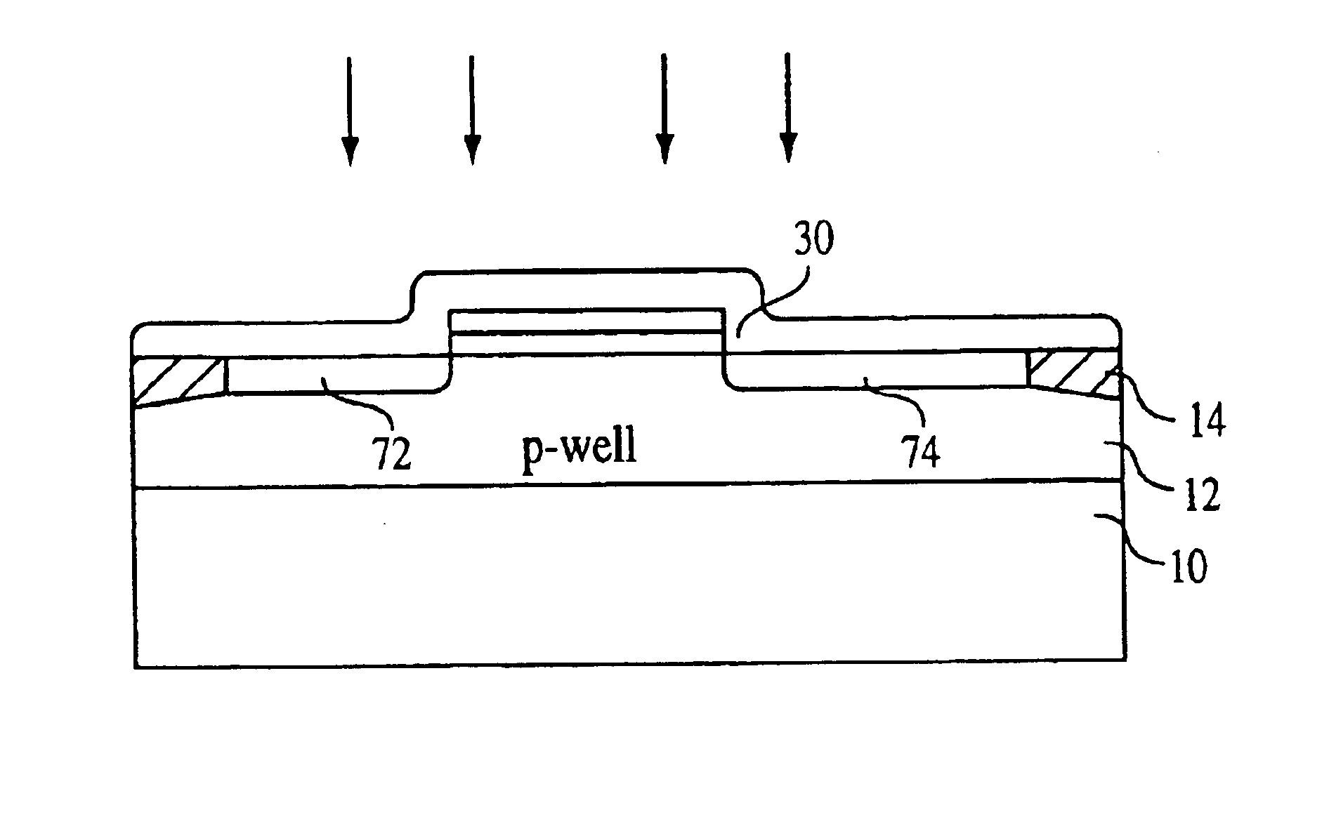
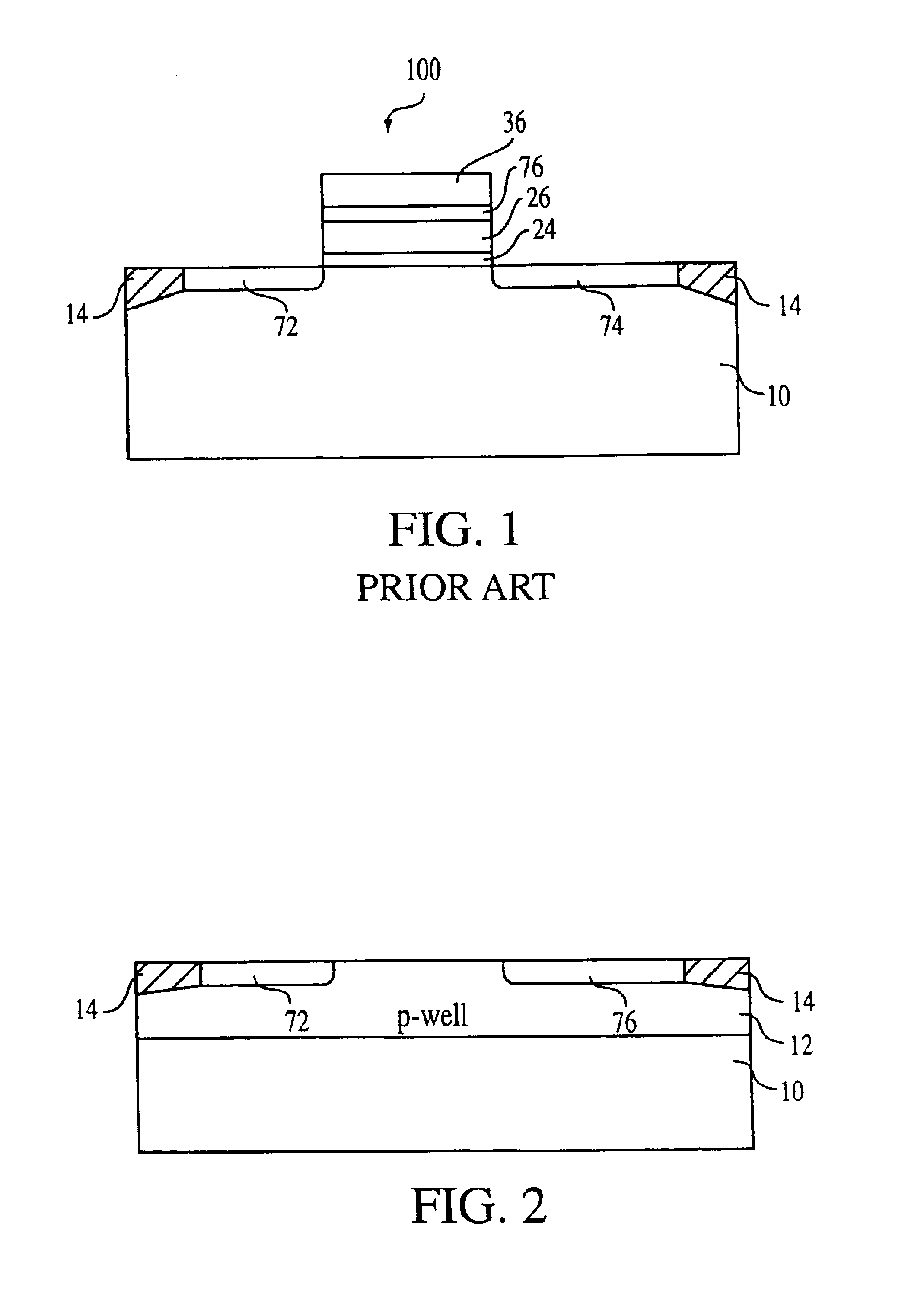
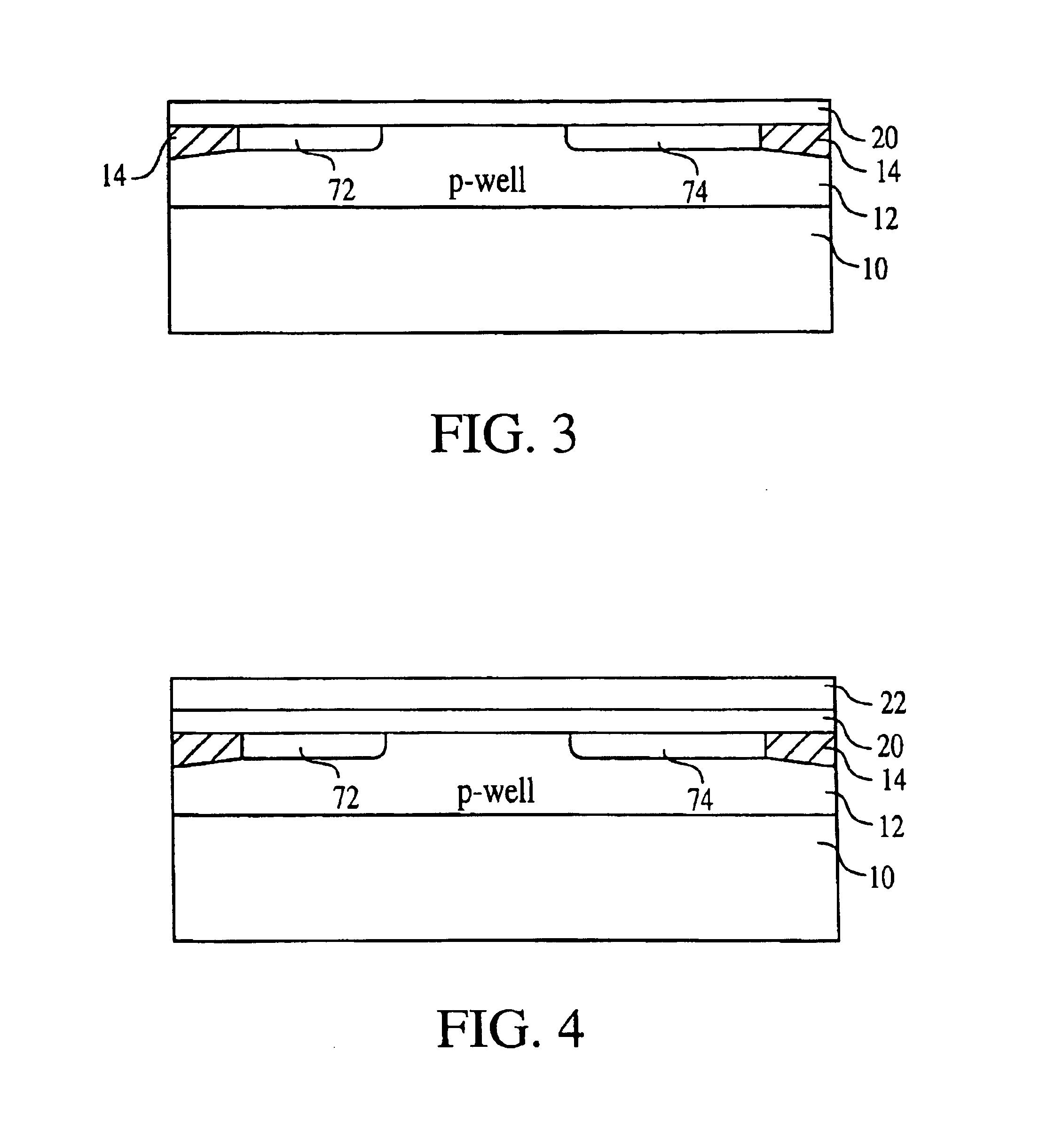
[0026]In the following detailed description, reference is made to various specific embodiments in which the invention may be practiced. These embodiments are described with sufficient detail to enable those skilled in the art to practice the invention, and it is to be understood that other embodiments may be employed, and that structural, logical, and electrical changes may be made.

[0027]The terms “wafer” or “substrate” used in the following description may include any semiconductor-based structure that has an exposed silicon surface. Wafer and structure must be understood to include silicon-on insulator (SOI), silicon-on sapphire (SOS), doped and undoped semiconductors, epitaxial layers of silicon supported by a base semiconductor foundation, and other semiconductor structures. The semiconductor need not be silicon-based. The semiconductor could be silicon-germanium, germanium, or gallium arsenide. When reference is made to a wafer or substrate in the following description, previou...


PUM


Abstract

A novel technique to quench electrical defects in CVD Al2O3 layers is disclosed. A small amount of silicon dopant to the aluminum oxide film reduces the leakage current as well as the gap interface trap density at the dielectric/silicon interface. The implanted silicon gives a better interface and improves the leakage characteristics of the dielectric.

Description

CROSS-REFERENCE TO RELATED APPLICATION[0001]This application is a divisional of application Ser. No. 09 / 532,086, filed on Mar. 21, 2000, now U.S. Pat. No. 6,750,502 which is hereby incorporated by reference.FIELD OF THE INVENTION[0002]The present invention relates generally to semiconductor circuits and, in particular, to a method for quenching defects in Al2O3 films.BACKGROUND OF THE INVENTION[0003]During the fabrication of metal-oxide-semiconductors (MOS), a silicon substrate is typically divided into a plurality of active and isolation regions through an isolation process. A thin gate oxide is subsequently grown on an upper surface of the substrate and over the active regions. A plurality of gates are then formed over the gate oxide layer, so that each gate bridges the substrate between doped source / drain regions. The source / drain regions are consequently implanted with an impurity concentration sufficient to render them conductive.[0004]MOS technology is greatly employed in the ...

Claims


Application Information

Patent Timeline
IPC IPC(8): H01L21/28H01L21/336H01L29/51H01L21/02H01L21/316H01L29/40
CPCH01L21/02145H01L21/02178H01L21/02271H01L21/02321H01L21/02351H01L21/28202H01L21/28273H01L21/3162H01L29/511H01L29/517H01L29/518H01L29/66825H01L29/40114
Inventor SANDHU, SUKESHPRALL, KIRK D.
Owner MICRON TECH INC
Why Eureka
Try Eureka