Transistor with variable electron affinity gate and methods of fabrication and use

a transistor and electron affinity technology, applied in transistors, semiconductor devices, instruments, etc., can solve the problems of large turn-on threshold voltage (vsub>t/sub>) magnitude, large tunneling barrier energy, and increase the time needed to store charge, so as to reduce the barrier energy, increase the tunneling probability of the sic gate, and accelerate the effect of programming and erasure tim

Inactive Publication Date: 2005-11-15
MICRON TECH INC
View PDF136 Cites 15 Cited by
  • Summary
  • Abstract
  • Description
  • Claims
  • Application Information

AI Technical Summary

Benefits of technology

[0013]In a flash electrically erasable and programmable read only memory (EEPROM) application, the SiC composition x is selected to provide the desired programming and erase voltage and time or data charge retention time. The lower barrier energy and increased tunneling probability of the SiC gate advantageously provides faster programming and erasure times for floating SiC gate transistors in flash EEPROM memories. This is particularly advantageous for “flash” EEPROMs in which many floating gate transistor memory cells must be erased simultaneously. Writing and erasure voltages are also advantageously reduced, minimizing the need for complicated and noisy on-chip charge pump circuits to generate the large erasure voltage. Lower erasure voltages also reduce hole injection into the gate dielectric that can cause erratic overerasure, damage to the gate dielectric, and introduction of trapping states in the gate dielectric. Reducing the erasure voltage also lowers the electric fields, minimizing reliability problems that can lead to device failure, and better accommodating downward scaling of device dimensions. Data charge retention time is decreased. Since conventional data charge retention times are longer than what is realistically needed, a shorter data charge retention time can be accommodated in order to obtain the benefits of a smaller barrier energy. The data charge retention time can be selected between seconds and millions of years by selecting the value of the SiC composition x, such as to obtain different memory functionality.

Problems solved by technology

For example, for p-channel FETs fabricated by a typical CMOS process, these and other material properties result in a large turn-on threshold voltage (VT) magnitude.
Conventional polysilicon gate FETs also have drawbacks that arise during use as a nonvolatile storage devices, such as in electrically erasable and programmable read only memories (EEPROMs).
However, the relatively large electron affinity of the polysilicon floating gate presents a relatively large tunneling barrier energy at its interface with the underlying gate dielectric.
The large tunneling barrier also increases the time needed to store charge on the polysilicon floating gates during the write operation and the time needed to remove charge from the polysilicon floating gate during the erase operation.
This is particularly problematic for “flash” EEPROMs, which have an architecture that allows the simultaneous erasure of many floating gate transistor memory cells.
Other problems result from the large erasure voltages that are typically applied to a control gate of the floating gate transistor in order to remove charge from the floating gate.
The large erasure voltages can result in hole injection into the gate dielectric.
This can cause erratic overerasure, damage to the gate dielectric, and introduction of trapping states in the gate dielectric.
The high electric fields that result from the large erasure voltages can also result in reliability problems, leading to device failure.
However, the absorption of photons in the semiconductor substrate is limited to high energy photons exceeding a bandgap energy of the semiconductor substrate.

Method used


Image

  • Transistor with variable electron affinity gate and methods of fabrication and use
  • Transistor with variable electron affinity gate and methods of fabrication and use
  • Transistor with variable electron affinity gate and methods of fabrication and use

Examples


Embodiment Construction

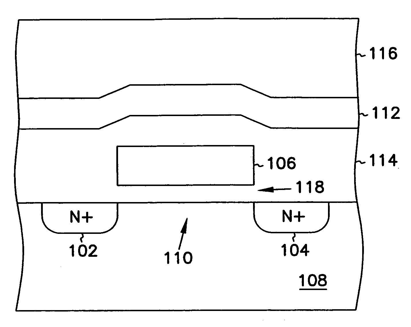
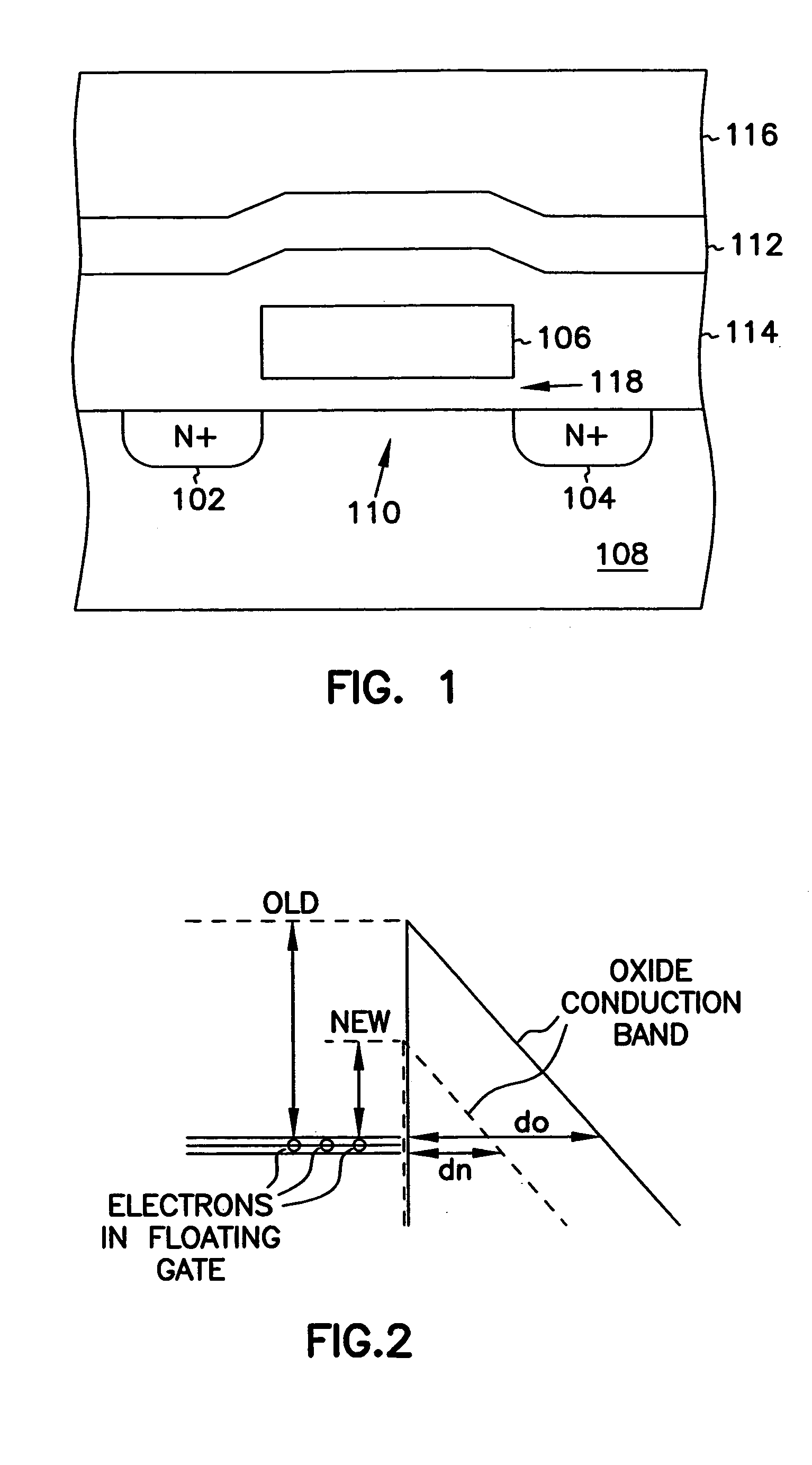
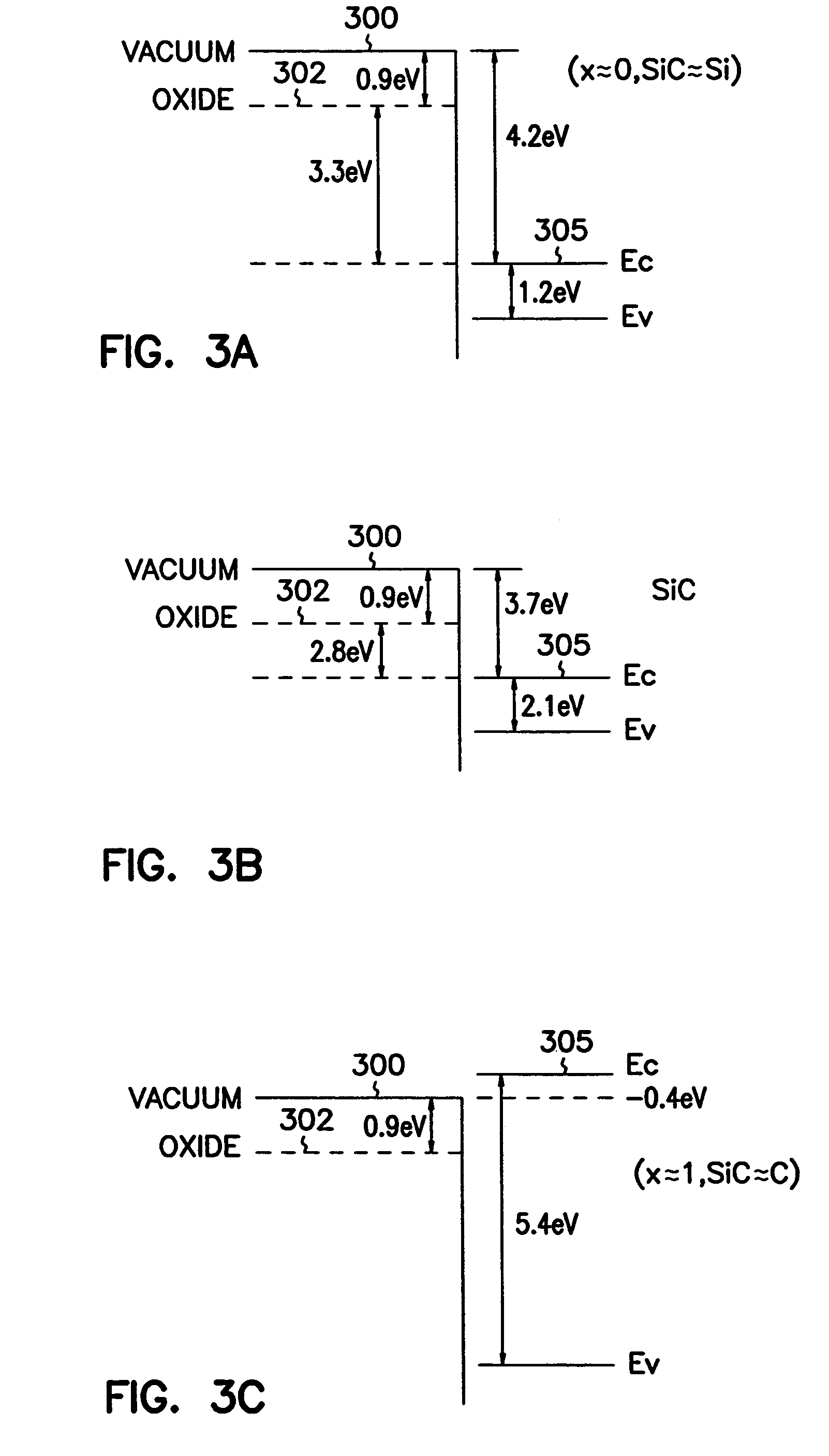
[0027]In the following detailed description of the invention, reference is made to the accompanying drawings which form a part hereof, and in which is shown, by way of illustration, specific embodiments in which the invention may be practiced. In the drawings, like numerals describe substantially similar components throughout the several views. The embodiments are described in sufficient detail to enable those skilled in the art to practice the invention. Other embodiments may be utilized and structural and electrical changes may be made without departing from the scope of the present invention. The terms wafer and substrate used in the following description include any semiconductor-based structure having an exposed surface with which to form the integrated circuit structure of the invention. Wafer and substrate are used interchangeably to refer to semiconductor structures during processing, and may include other layers that have been fabricated thereupon. Both wafer and substrate ...


PUM


Abstract

A CMOS-compatible FET has a reduced electron affinity polycrystalline or microcrystalline SiC gate that is electrically isolated (floating) or interconnected. The SiC material composition is selected to establish the barrier energy between the SiC gate and a gate insulator. In a memory application, such as a flash EEPROM, the SiC composition is selected to establish a lower barrier energy to reduce write and erase voltages and times or accommodate the particular data charge retention time needed for the particular application. In a light detector or imaging application, the SiC composition is selected to provide sensitivity to the desired wavelength of light. Unlike conventional photodetectors, light is absorbed in the floating gate, thereby ejecting previously stored electrons therefrom. Also unlike conventional photodetectors, the light detector according to the present invention is actually more sensitive to lower energy photons as the semiconductor bandgap is increased.

Description

[0001]This application is a continuation of U.S. Ser. No. 08 / 903,452, filed on Jul. 29, 1997, now abandoned.FIELD OF THE INVENTION[0002]The present invention relates generally to integrated circuit technology, and particularly to a silicon carbide gate transistor, such as a floating gate transistor, and complementary metal-oxide-semiconductor (CMOS) compatible methods of fabrication, and methods of use in memory and light detection devices.BACKGROUND OF THE INVENTION[0003]Field-effect transistors (FETs) are typically produced using a standard complementary metal-oxide-semiconductor (CMOS) integrated circuit fabrication process. Such a process allows a high degree of integration for obtaining high circuit density with relatively few processing steps. Resulting FETs typically have gate electrodes composed of n-type conductively doped polycrystalline silicon (polysilicon) material.[0004]The intrinsic properties of the polysilicon gate material affects operating characteristics of the F...

Claims


Application Information

Patent Timeline
Patent Type & Authority Patents(United States)
IPC IPC(8): H01L21/28H01L29/40H01L29/423H01L21/02H01L29/49
CPCH01L21/2807H01L21/28273H01L29/42324H01L29/4983H01L31/113H01L29/40114
Inventor FORBES, LEONARDAHN, KIE Y.
Owner MICRON TECH INC
Why Eureka
Try Eureka