Thermal annealing for Cu seed layer enhancement

a technology of cu alloy and enhancement layer, which is applied in the direction of semiconductor devices, basic electric elements, electrical equipment, etc., can solve the problems of reducing production throughput, increasing the rxc delay caused by the interconnect wiring, and severe requirements for semiconductor fabrication technology, etc., to reduce voids, enhance the film, and reduce the resistance of cu or cu alloy interconnects

Inactive Publication Date: 2006-02-14
ADVANCED MICRO DEVICES INC
View PDF7 Cites 28 Cited by
  • Summary
  • Abstract
  • Description
  • Claims
  • Application Information

AI Technical Summary

Benefits of technology

[0011]An advantage of the present invention is a method of manufacturing a semiconductor device having reliable, low resistance Cu or Cu alloy interconnects with significantly reduced voids.
[0012]Additional advantages and other features of the present invention will be set forth in the description which follows and, in part, will become apparent to those having ordinary skill in the art upon examination of the following or may be learned from the practice of the present invention. The advantages of the present invention may be realized and obtained as particularly pointed out in the appended claims.
[0013]According to the present invention, the foregoing and other advantages are achieved in part by a method of manufacturing a semiconductor device, the method comprising: forming an opening in a dielectric layer; depositing a barrier layer lining the opening; depositing a seed layer for copper (Cu) or Cu alloy deposition on the barrier layer; depositing a conformal seed layer enhancement film by electroplating on the seed layer; thermal annealing the seed layer enhancement film; and filling the opening with Cu or a Cu alloy.
[0014]Embodiments include forming a dual damascene opening in dielectric material having a dielectric constant no greater than about 3.9, such as a fluorine (F)-containing oxide, such as an F-containing oxide derived from tetraethyl orthosilicate (TEOS), the opening comprising an upper trench section in communication with a lower via hole section; depositing a composite barrier layer lining the opening, the composite barrier layer comprising a layer of tantalum nitride and a layer of α-tantalum thereon; depositing a seed layer by PVD on the α-tantalum layer, the deposited seed layer having discontinuities, depositing a conformal seed layer enhancement film by electroplating bridging discontinuities in the seed layer and having a rough surface; thermal annealing the seed layer enhancement film by heating, as in a furnace or by lamp annealing, in an inert atmosphere, such as nitrogen or argon, or in a reducing gas atmosphere, such as a forming gas comprising hydrogen and nitrogen, to reduce the roughness and resistivity of the seed layer enhancement film; and filling the opening with Cu or a Cu alloy to form a Cu or Cu alloy line in communication with an underlying Cu or Cu alloy via. Embodiments of the present invention include annealing by heating in a furnace to a temperature of about 100° C. to about 250° C. for about 1 minute to about 30 minutes.

Problems solved by technology

The escalating demand for high density and performance impose severe requirements on semiconductor fabrication technology, particularly interconnection technology in terms of providing reliable low RxC (resistance x capacitance) interconnect patterns with higher electromigration resistance, wherein sub-micron vias, contacts and trenches have high aspect ratios.
As the length of metal interconnects increases and cross-sectional areas and distances between interconnects decrease, the RxC delay caused by the interconnect wiring increases.
As design rules are reduced to about 0.12 micron and below, the rejection rate due to integrated circuit speed delays significantly reduces production throughput and increases manufacturing costs.
In implementing Cu metallization, particularly in damascene techniques wherein an opening is formed in a dielectric layer, particularly a dielectric layer having a low dielectric constant, e.g., a dielectric constant less than about 3.9, various reliability, electromigration and resistance issues are generated.
Reliability issues stem, in part, from the difficulty in forming a continuous seed layer on a barrier layer in an opening, particularly as the feature sizes continue to shrink into the deep sub-micron regime.
As a result of reduced feature sizes and high aspect ratios, it is extremely difficult to deposit a continuous seed layer lining the sidewalls of the opening.
In addition, it is even difficult to effectively plate the seed layer 12 on the bottom of the opening.
Consequently, voids are induced leading to high resistance vias and lines or open circuits.
However, it was found that such seed layer enhancement films exhibit poor properties, such as an undesirable surface roughness, e.g., an average surface roughness (Ra) greater than 25 Å vis-à-vis an Ra of 5 Å to 7 Å for a conventionally deposited PVD Cu film.
It was also found that such a seed layer enhancement film 20 not only exhibits an undesirable surface roughness but also undesirably high impurity concentrations of elements such as carbon, oxygen, nitrogen and hydrogen.
As a result, the subsequently deposited electroplated Cu film exhibits high resistivity, high surface roughness and voids, leading to significantly increased via / line resistance and lower circuit speed, in addition to generating electromigration and other reliability issues.

Method used


Image

  • Thermal annealing for Cu seed layer enhancement
  • Thermal annealing for Cu seed layer enhancement
  • Thermal annealing for Cu seed layer enhancement

Examples


Embodiment Construction

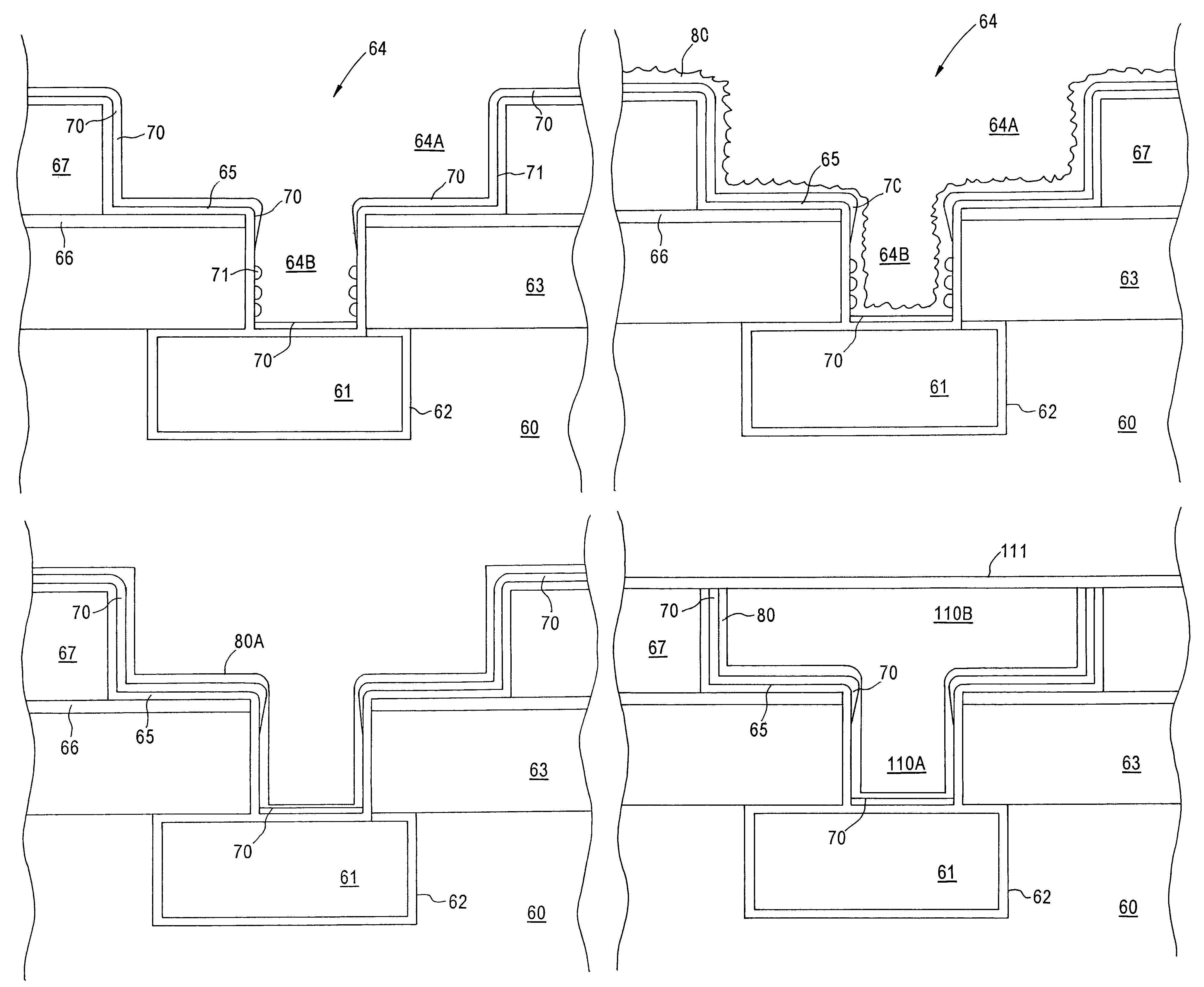
[0019]The present invention addresses and solves various problems attendant upon forming metallized interconnects, such as Cu or Cu alloy interconnects, particularly, damascene structures in dielectric layer(s) having a dielectric constant less than about 3.9. As employed throughout this application, the symbol Cu is intended to encompass high purity elemental copper as well as Cu-based alloys, such as Cu alloys containing minor amounts of tantalum, indium, tin, zinc, manganese, titanium, magnesium, chromium, titanium, germanium, strontium, platinum, magnesium, aluminum or zirconium.

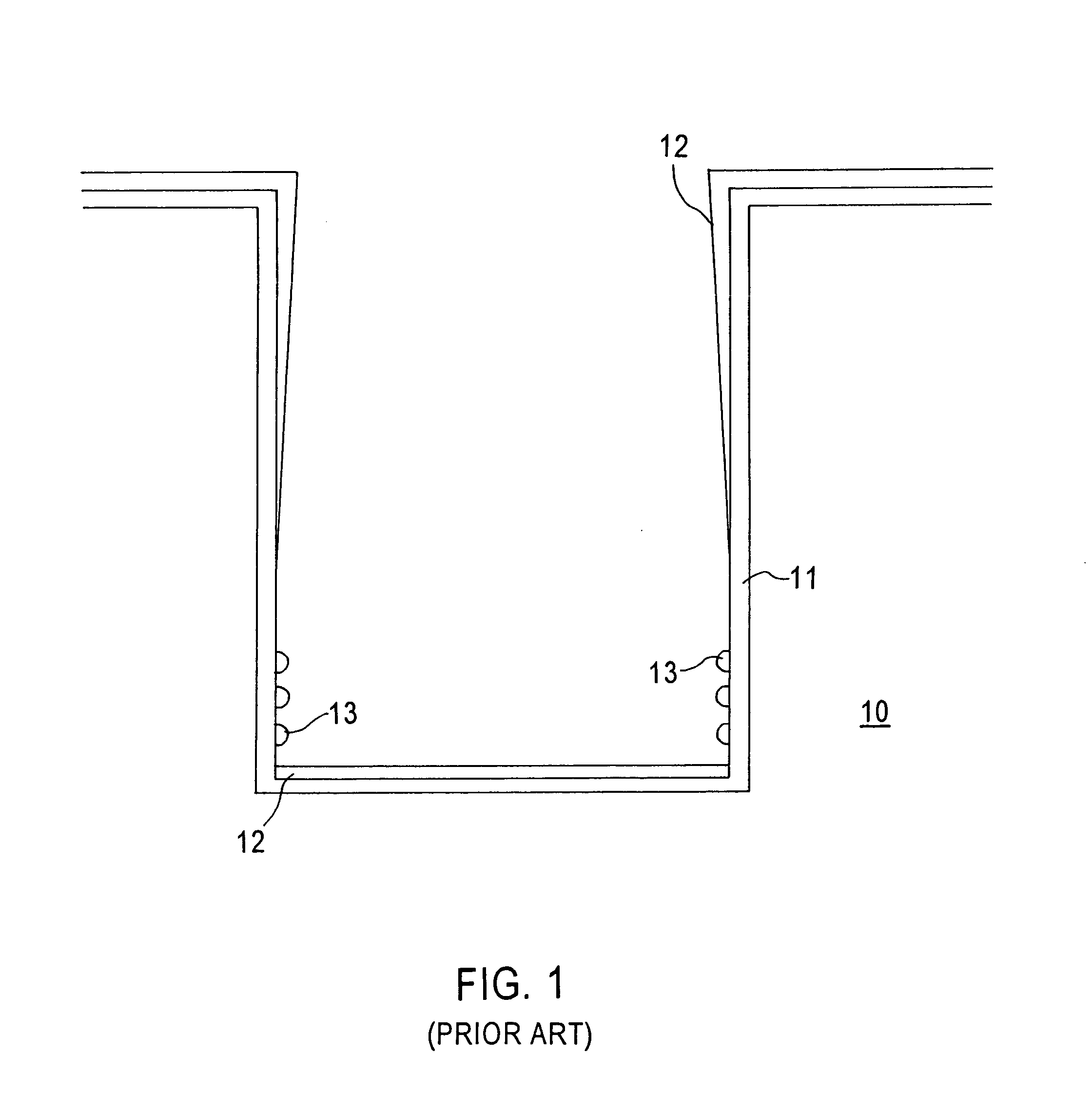
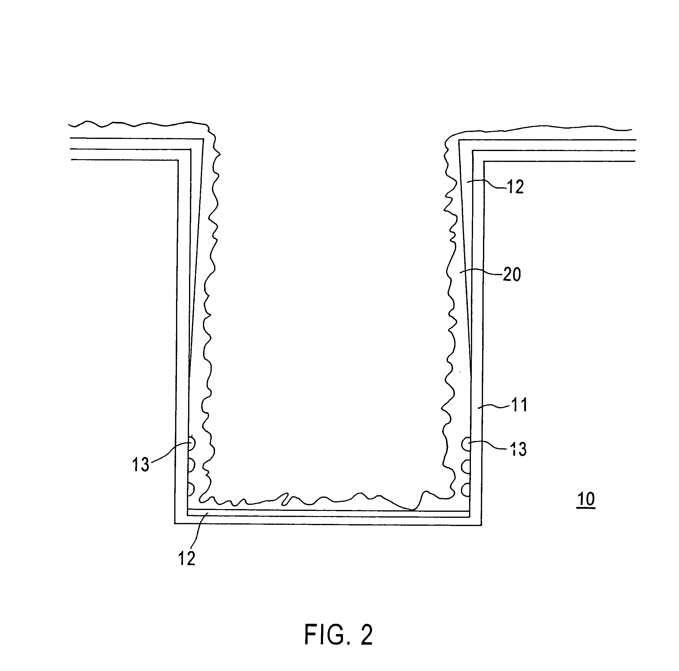
[0020]As design rules are scaled down into the deep sub-micron range, such as about 0.12 micron and under, reliability and contact resistance issues associated with interconnects, particularly Cu interconnects, become increasingly significant. Reliability and contact resistance issues stem, in part, from the inability to deposit a continuous seed layer for Cu deposition, particularly as the dimensions sh...


PUM

PropertyMeasurementUnit
temperatureaaaaaaaaaa
dielectric constantaaaaaaaaaa
temperatureaaaaaaaaaa

Abstract

Semiconductor devices with highly reliable Cu interconnects exhibiting reduced resistance are formed by sequentially depositing a seed layer by PVD, depositing a conformal seed layer enhancement film by electroplating, and then thermal annealing the seed layer enhancement film in an inert or reducing atmosphere to expel impurities, enhance film conductivity, reduce film stress, increase film density, and reduce film roughness. Embodiments include single and dual Cu damascene techniques formed in dielectric layers having a dielectric constant no greater than about 3.9.

Description

FIELD OF THE INVENTION[0001]The present invention relates to copper (Cu) and / or Cu alloy metallization in semiconductor devices, and to a method for manufacturing semiconductor devices with reliable, low resistance Cu or Cu alloy interconnects. The present invention is particularly applicable to manufacturing high speed integrated circuits having sub-micron design features and high conductivity interconnect structures.BACKGROUND ART[0002]The escalating demand for high density and performance impose severe requirements on semiconductor fabrication technology, particularly interconnection technology in terms of providing reliable low RxC (resistance x capacitance) interconnect patterns with higher electromigration resistance, wherein sub-micron vias, contacts and trenches have high aspect ratios.[0003]Conventional semiconductor devices comprise a semiconductor substrate, typically doped monocrystalline silicon, and a plurality of sequentially formed interlayer dielectrics and conducti...

Claims


Application Information

Patent Timeline
Patent Type & Authority Patents(United States)
IPC IPC(8): H01L21/44H01L21/4763
CPCH01L21/2885H01L21/76843H01L21/76868H01L21/76873H01L21/76864H01L2221/1089
Inventor TRAN, MINH Q.
Owner ADVANCED MICRO DEVICES INC
Why Eureka
Try Eureka