Coating of copper and silver air bridge structures to improve electromigration resistance and other applications

a technology of air bridge and copper, applied in the field of integrated circuits, can solve the problems of increasing the number of electrical interconnects of high-density devices, increasing signal propagation delays and signal cross-talk, and increasing the number of circuit elements of high-density devices, so as to reduce the electromigration rate of copper, reduce the effect of surface diffusion, and reduce the effect of solubility

Inactive Publication Date: 2006-05-23
MICRON TECH INC
View PDF12 Cites 2 Cited by
  • Summary
  • Abstract
  • Description
  • Claims
  • Application Information

AI Technical Summary

Benefits of technology

[0020]The aforementioned needs are satisfied by one aspect of the present invention which discloses a method and device for forming an electrical interconnect comprising an air bridge structure for electrically connecting at least two circuit elements in an integrated circuit. In order to reduce the electromigration rate of the copper or any other sub-micron conductor it will be necessary to find ways to reduce the effect of surface diffusion on the electromigration rate. This can be accomplished by coating the surface of the conductor with a thin highly adhesive coating, which has a low solubili...

Problems solved by technology

However, as circuit density is increased, problems associated with conventional electrical interconnects are becoming more apparent.
In particular, a higher density device having an increased number of circuit elements will likely require an even greater increase in the number of electrical interconnects.
Unfortunately, such dimensional reductions tend to increase the resistance of individual interconnects and increase the capacitance between adjacent interconnects, thereby possibly increasing signal propagation delays and signal cross-talk.
Hence, while it is desirable to increase device density on integrated circuits, considerations such as these pose problems for maintaining or improving circuit performance.
However, several potential problems have been encountered in the development of this proposed metallurgy.
Fast diffusion of copper into silicon or silicon oxide results in diffusion of the conductive interconnect into the surrounding materials which can damage device performance or can result in short circuits occurring between adjacent interconnects.
However, as in the case of SiO2, an incompatibility problem with copper metallurgy has been found.
A primary difficulty that results is the relative incompatibility of lower resistance materials with the surrounding insulating material.
However, the use of a vacuum introduces additional problems or complexities to the device.
The first being the low heat conductivity of the vacuum and the second being the cost of the package required to maintain the vacuum.
Air, which has somewhat better thermal conductivity, has its own problems in that both copper and silver react with air to form oxides or other compounds.
However, because the air bridge tends to sag under its own weight, the length of the air bridge is a possible limiting factor.
In particular, because the air bridge is only supported at its first and second en...

Method used


Image

  • Coating of copper and silver air bridge structures to improve electromigration resistance and other applications
  • Coating of copper and silver air bridge structures to improve electromigration resistance and other applications
  • Coating of copper and silver air bridge structures to improve electromigration resistance and other applications

Examples


Embodiment Construction

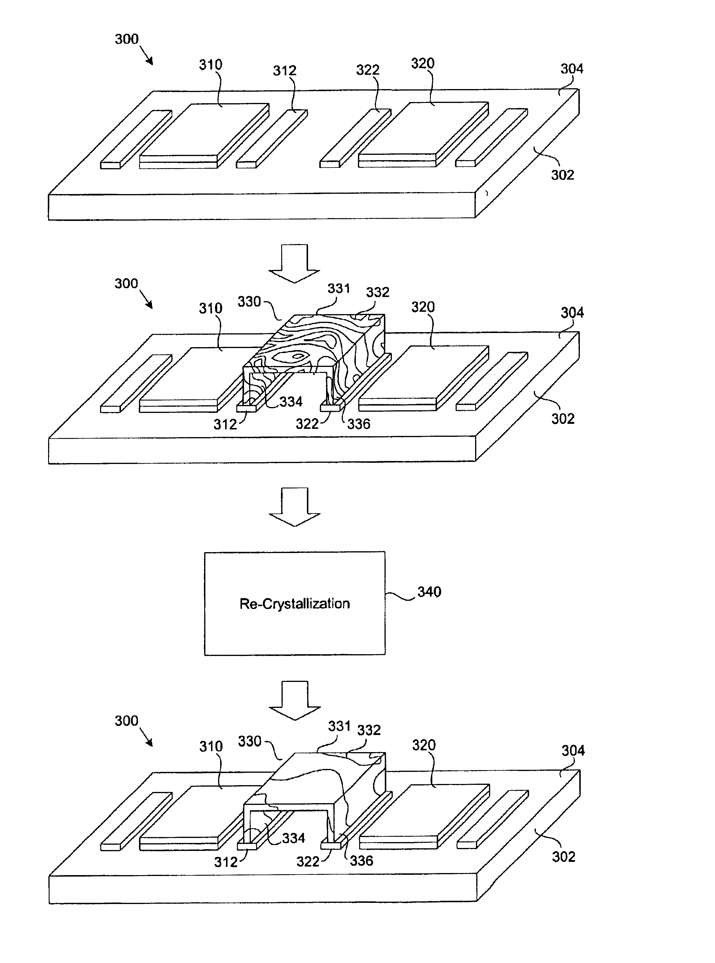
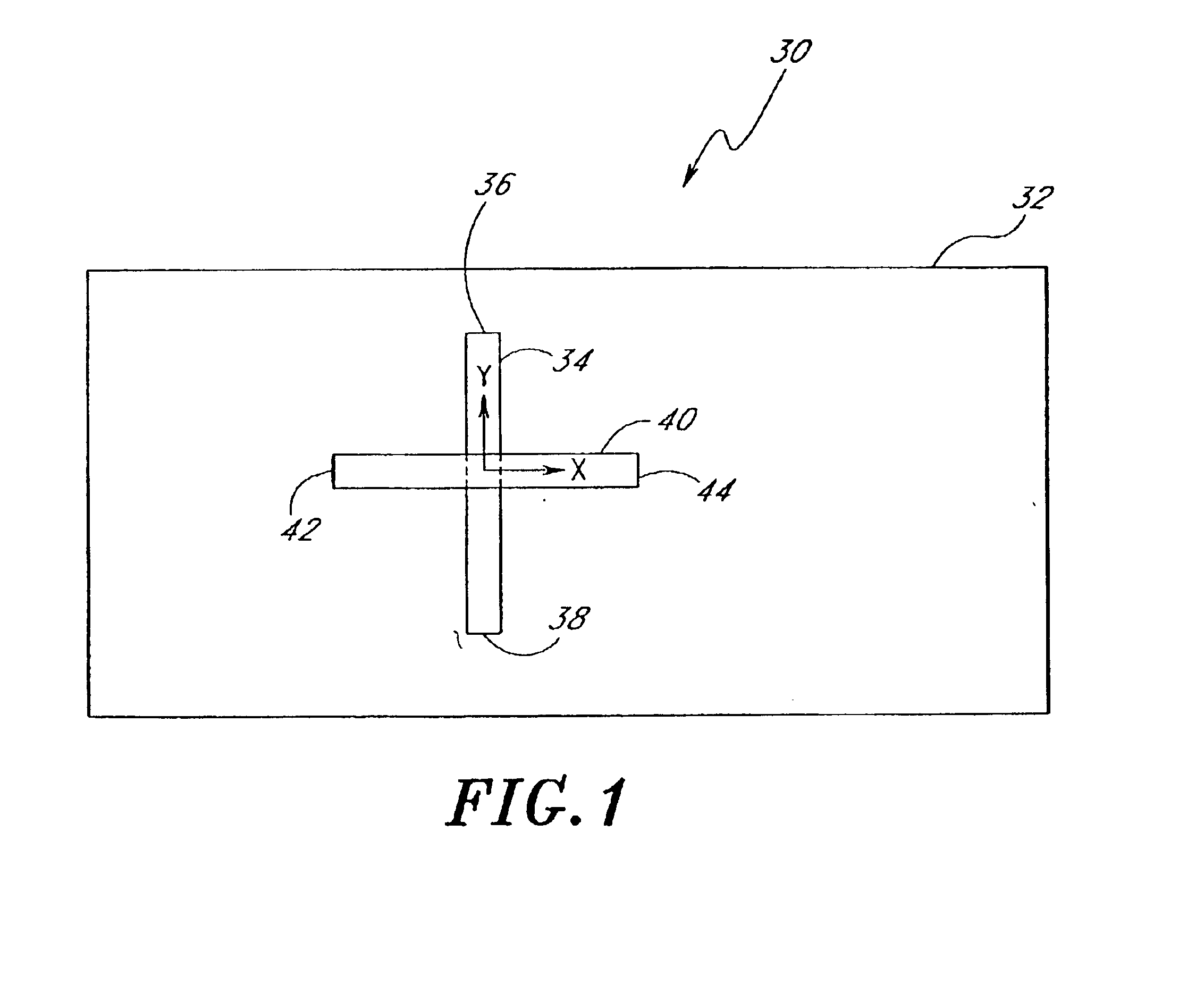
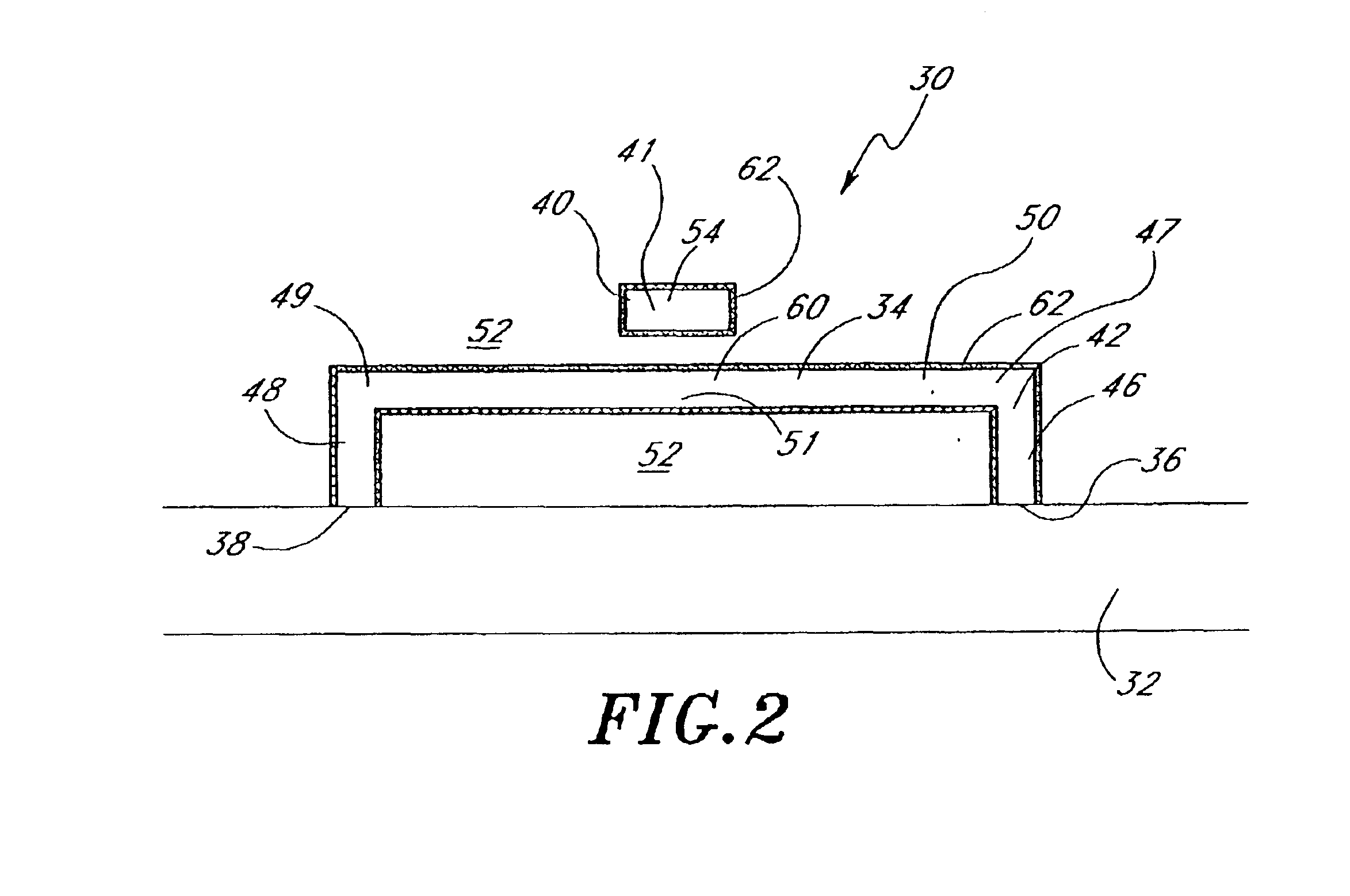
[0039]The illustrated embodiments of the present invention comprise a miniaturized electrical interconnect having improved operating characteristics and methods for providing the same. The electrical interconnect includes a bridge section surrounded by air, referred to hereinbelow as an “air bridge”, so as to reduce the capacitance of the interconnect. Air bridges are also described in U.S. Pat. No. 5,891,797 which is incorporated herein by reference in its entirety. As will be described in greater detail below, air bridges formed in accordance with the various aspects of the present invention are provided with reduced resistance and a reduced tendency to sag, thereby enabling them to have a reduced cross-sectional area and to extend across larger distances.

[0040]Improved electrical interconnects formed according to the methods of the illustrated embodiments are particularly useful in the manufacture of ultra-high density integrated circuit devices, such as a Dynamic Random Access M...


PUM


Abstract

An improved electrical interconnect for an integrated circuit and methods for providing the same are disclosed. The electrical interconnect includes an air bridge extending through a gaseous medium so as to reduce the capacitance of the interconnect. The air bridge is supported at a first and second end such that the air bridge is suspended above the substrate. The air bridge comprises a highly conductive material, such as silver, so as to provide the air bridge with a reduced resistivity. To inhibit gaseous medium from contaminating the air bridge, the air bridge further comprises an adherent coating interposed between the air bridge and the gaseous medium. A method of forming the electrical interconnect is also disclosed, wherein, prior to forming the adherent coating, the conductive material is processed so as to form fewer grain boundaries, which enhances the electrical properties of the air bridge.

Description

BACKGROUND OF THE INVENTION[0001]1. Field of the Invention[0002]The present invention relates to integrated circuits and, in particular, relates to miniaturized electrical interconnects having reduced resistance and capacitance.[0003]2. Description of the Related Art[0004]To provide improved performance, manufacturers of integrated circuit devices continually strive to increase circuit density. Such devices are typically formed on a semiconductor substrate, such as a silicon wafer, and comprise a large number of miniaturized circuit elements. These elements, which include transistors, diodes, capacitors, and resistors, are usually disposed within or adjacent the substrate and define a plurality of circuit nodes. To combine the circuit elements into a useful electronic circuit, integrated circuit devices typically include a plurality of conducting paths that link the circuit nodes in a preferred manner. Typically, the conducting paths are provided by electrical interconnects comprisi...

Claims


Application Information

Patent Timeline
IPC IPC(8): H01L21/4763
CPCH01L21/7682H01L21/76834H01L21/76838H01L21/7685H01L21/76852H01L23/5221H01L23/5222H01L2924/0002H01L2924/00
Inventor FARRAR, PAUL A.
Owner MICRON TECH INC
Why Eureka
Try Eureka