Apparatus for processing a semiconductor
- Summary
- Abstract
- Description
- Claims
- Application Information
AI Technical Summary
Benefits of technology
Problems solved by technology
Method used
Image

Examples
example 1
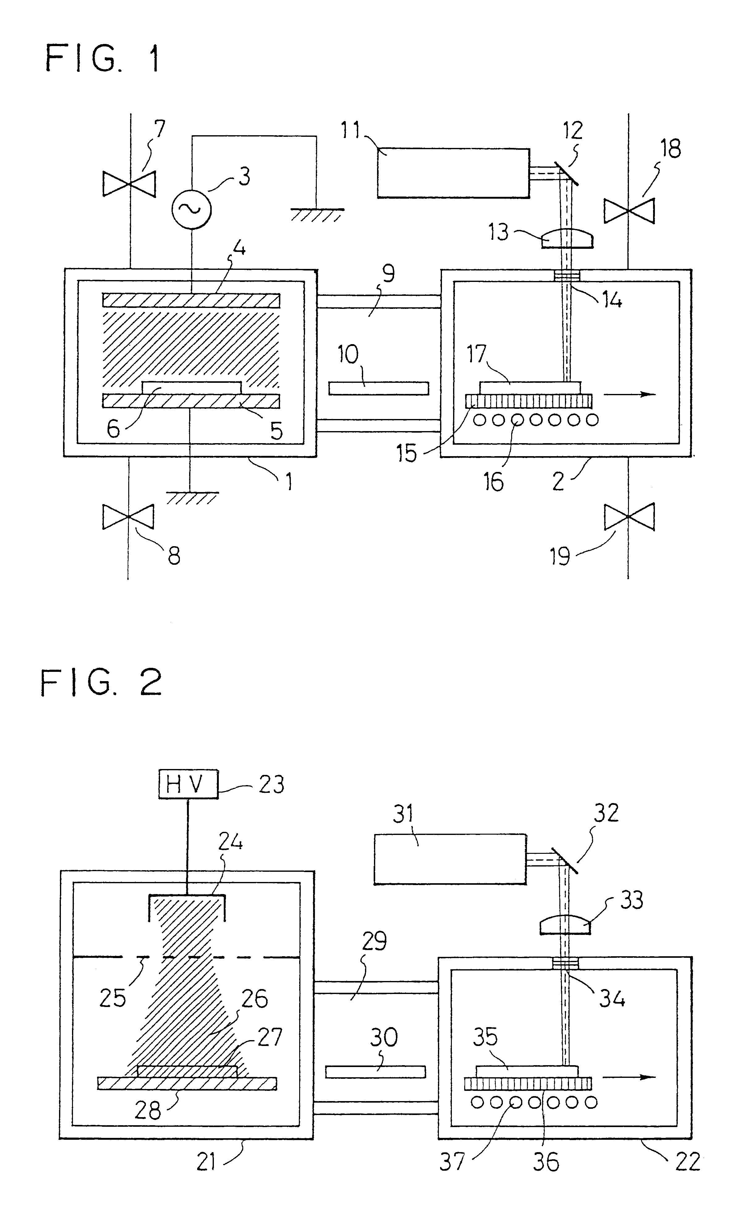
[0017]Referring to FIG. 1, there is shown a multi-chamber system according to the invention. This multi-chamber system comprises a plasma CVD film formation apparatus and a laser processing apparatus (e.g., a laser annealing apparatus). A preliminary chamber is formed between these two apparatuses. The plasma CVD apparatus has a chamber 1 equipped with a gas intake valve 7 and an exhaust valve 8. The laser annealing apparatus has a chamber 2 equipped with a gas intake valve 18 and an exhaust valve 19. These valves permit requisite gases to go into and out of these chambers. Also, these valves make it possible to maintain the pressure inside each chamber at an appropriate value.
[0018]The chamber 1 is further equipped with electrodes 4 and 5. A substrate or sample 6 to be processed is placed on the electrode 5. An RF power supply 3 of frequency, for example, of 13.56 MHz is connected with the electrode 4. An adequate gas such as monosilane or disilane is admitted into the chamber to i...
example 2
[0024]Referring to FIG. 2, there is shown another multi-chamber system according to the invention. This system comprises a combination of a plasma doping apparatus and a laser processing apparatus (e.g., a laser annealing apparatus). A preliminary chamber is formed between these two apparatuses.
[0025]The plasma doping apparatus and the laser annealing apparatus have chambers 21 and 22, respectively. These chambers are designed so that requisite gases can be introduced into them and that unwanted gases can be expelled from them. Also, the pressure inside each chamber can be maintained at an appropriate value.
[0026]The chamber 21 is further equipped with an anode electrode 24 and a grid electrode 25. A high voltage which can be increased up to 100 kV is applied to the anode from a high voltage source 23. A plasma is produced around the grid electrode by RF discharge and contains positive ions 26. These ions 26 are accelerated toward a sample holder 28 by the high voltage described abo...
example 3
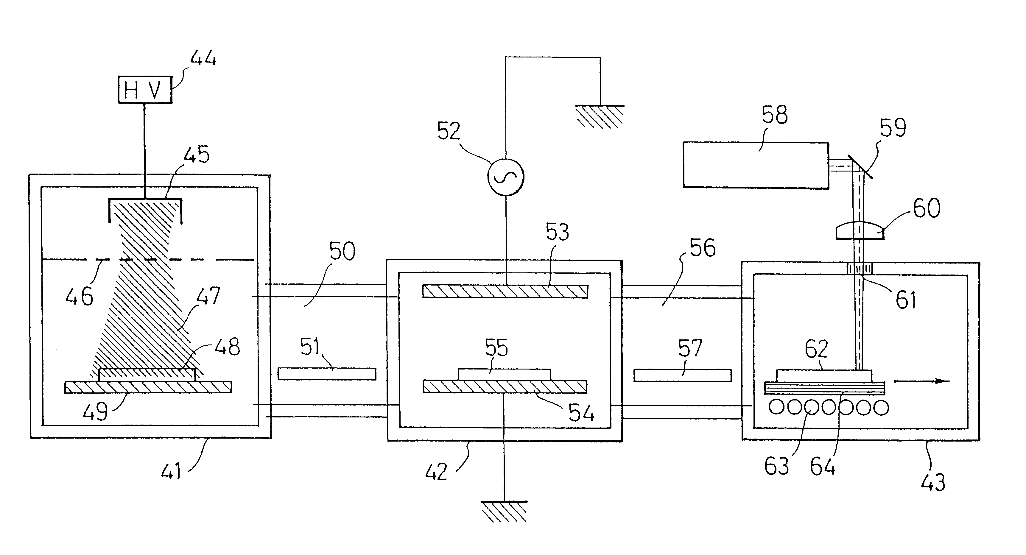
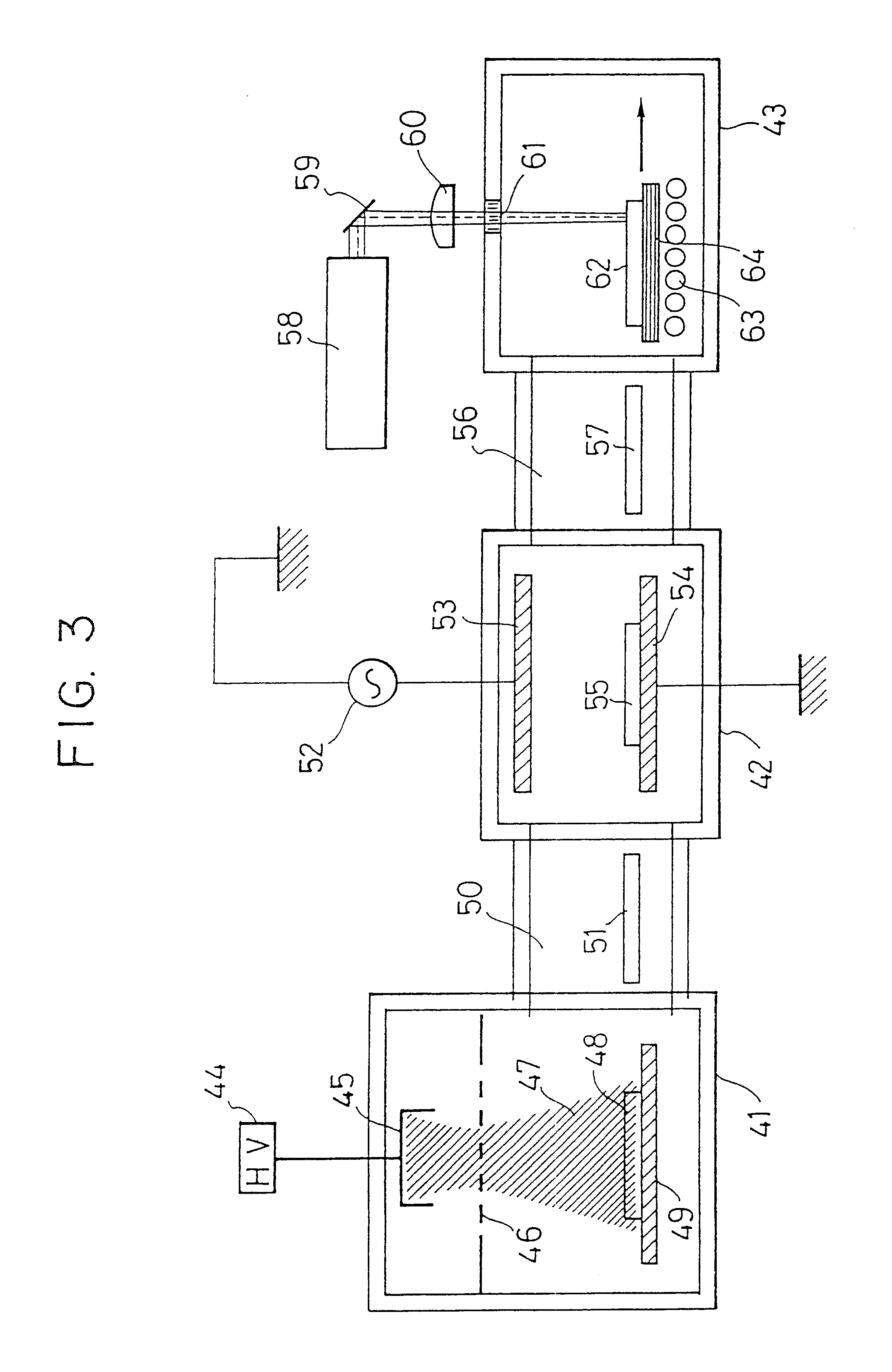
[0029]Referring next to FIG. 3, there is shown a further multi-chamber system according to the invention. This system comprises a combination of a plasma doping apparatus, a dry etching apparatus, and a laser processing apparatus (e.g., a laser annealing apparatus). A preliminary chamber is formed between any adjacent ones of these three apparatuses.
[0030]The plasma doping apparatus, the etching apparatus, and the laser annealing apparatus have chambers 41, 42, and 43, respectively. These chambers are designed so that requisite gases can be introduced into them and that unwanted gases can be discharged from them. Also, the pressure inside each chamber can be maintained at an appropriate value.
[0031]The chamber 41 is further equipped with an anode electrode 45 and a grid electrode 46. A high voltage which can be increased up to 100 kV is applied to the anode from a high voltage source 44. A plasma is produced around the grid electrode by RF discharge and contains positive ions 47. Th...
PUM
| Property | Measurement | Unit |
|---|---|---|
| Length | aaaaa | aaaaa |
| Length | aaaaa | aaaaa |
| Wavelength | aaaaa | aaaaa |
Abstract
Description
Claims
Application Information