Method of fabricating a semiconductor device utilizing a catalyst material solution

Inactive Publication Date: 2007-03-06
SEMICON ENERGY LAB CO LTD
View PDF166 Cites 15 Cited by
  • Summary
  • Abstract
  • Description
  • Claims
  • Application Information

AI Technical Summary

Benefits of technology

[0065]Further, to improve the crystallization ratio, the step of applying laser light or strong light and the heat treatment step for reducing defects in a film may alternately be repeated two or more times.
[0066]According to the present invention, by virtue of the effect of an interstitial element for accelerating crystallization, the crystallization of an amorphous silicon film can be performed at a low temperature in a short time. Specifically, the invention enables manufacture of a crystalline silicon film by a heat treatment of 550° C. and about 4 hours, which was impossible conventionally. An interstitial element with respect to silicon accelerates crystallization as it diffuses through a silicon film. Therefore, a crystalline silicon film can be obtained which does not have definite crystal grain boundaries,

Problems solved by technology

Although an amorphous silicon film is conveniently used for the TFTs, it has a problem of low-grade electrical characteristics.
However, since the crystallization by heating takes more than 20 hours at a heating temperature higher than 600° C., it is difficult to use a glass substrate.
For example, Corning 7059 glass, which is used for active liquid crystal display devices, has a glass strain point of 593° C. Therefore, as the size of a substrate becomes larger, heating at more than 600° C. will be problematic.
Further, when an amorphous silicon film is crystallized by heating, the entire silicon film is crystallized; that is, it is impossible to effect partial crystallization nor control the crystallinity of a particular region.
Although Al and Sn, which are substitutional metal element with respect to silicon, are effective in generating initial nuclei, they are not effective in crystal growth that should follow.
Therefore, even if Al or Sn is used, the crystallizat

Method used


Image

  • Method of fabricating a semiconductor device utilizing a catalyst material solution
  • Method of fabricating a semiconductor device utilizing a catalyst material solution
  • Method of fabricating a semiconductor device utilizing a catalyst material solution

Examples


Example

Embodiment 1

[0079]In this embodiment, to impart crystallinity to an amorphous silicon film, an aqueous solution containing a catalyst element for accelerating crystallization is applied to the amorphous silicon film, and then laser light irradiation is performed.

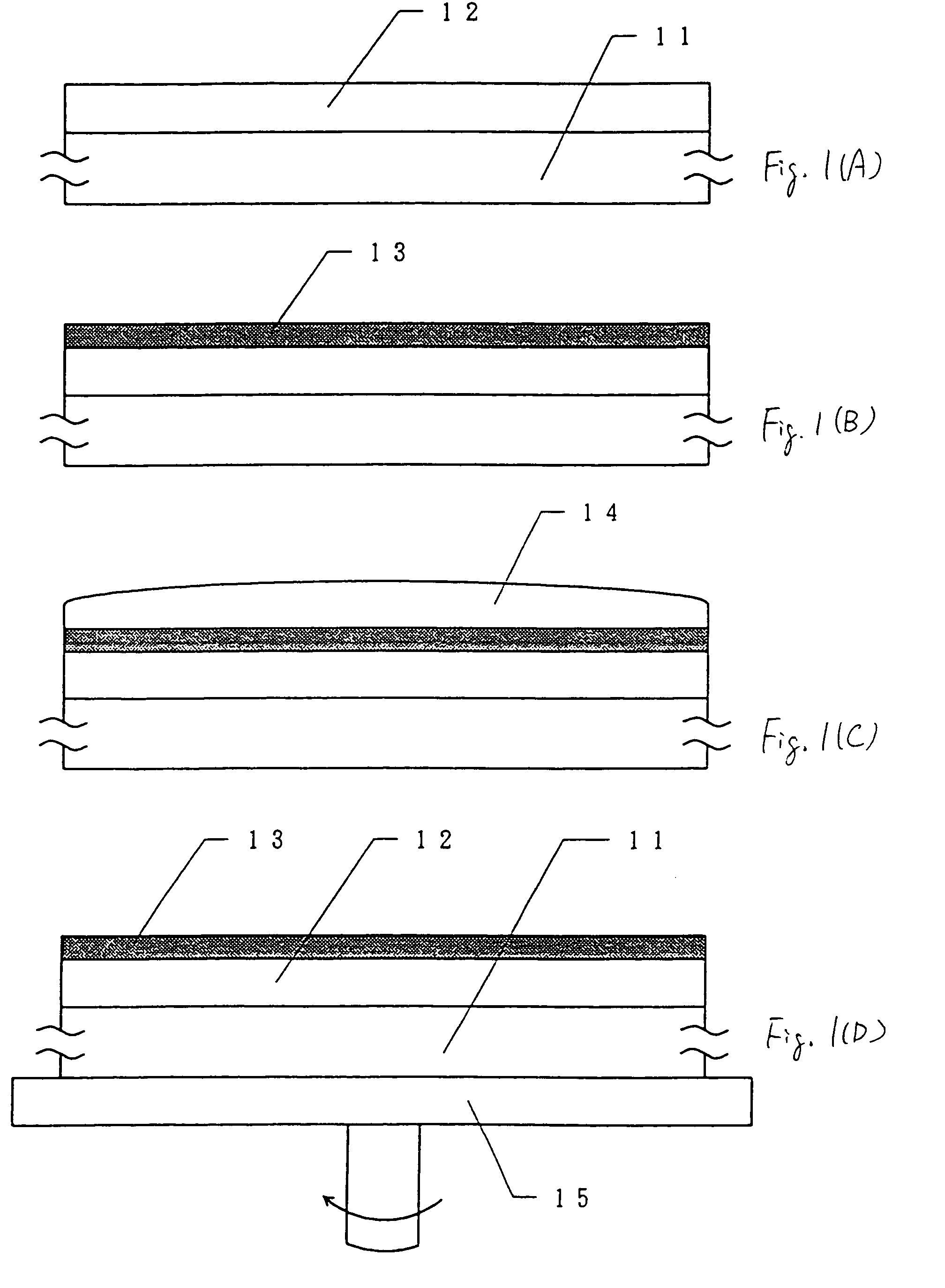
[0080]Referring to FIGS. 1(A) to 1(D), steps to the introduction of a catalyst element (nickel in this embodiment) will be described. In this embodiment, a plate of Corning 7059 glass having a size of 100 mm×100 mm is used as a substrate 11.

[0081]First, an amorphous silicon film of 100 to 1,500 Å in thickness is deposited by plasma CVD or LPCVD. In this embodiment, a 1,000-Å-thick amorphous silicon film 12 is deposited by plasma CVD. (FIG. 1(A))

[0082]Then, a hydrofluoric acid treatment is performed to remove stain and a natural oxide film, and an oxide film 13 of 10 to 50 Å in thickness is formed. Where stain is negligible, the natural oxide film itself may be used instead of the oxide film 13. (FIG. 1(B))

[0083]Since the oxi...

Example

Embodiment 2

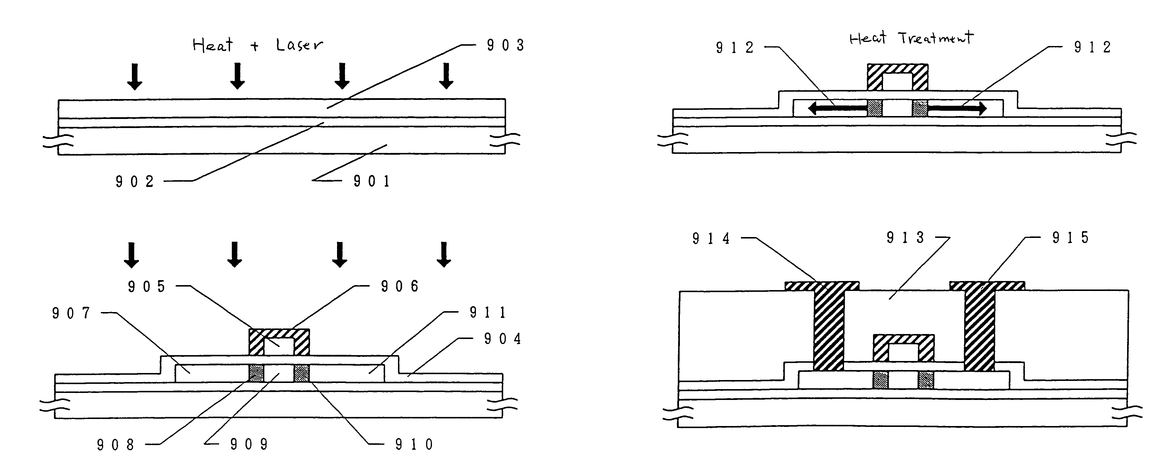
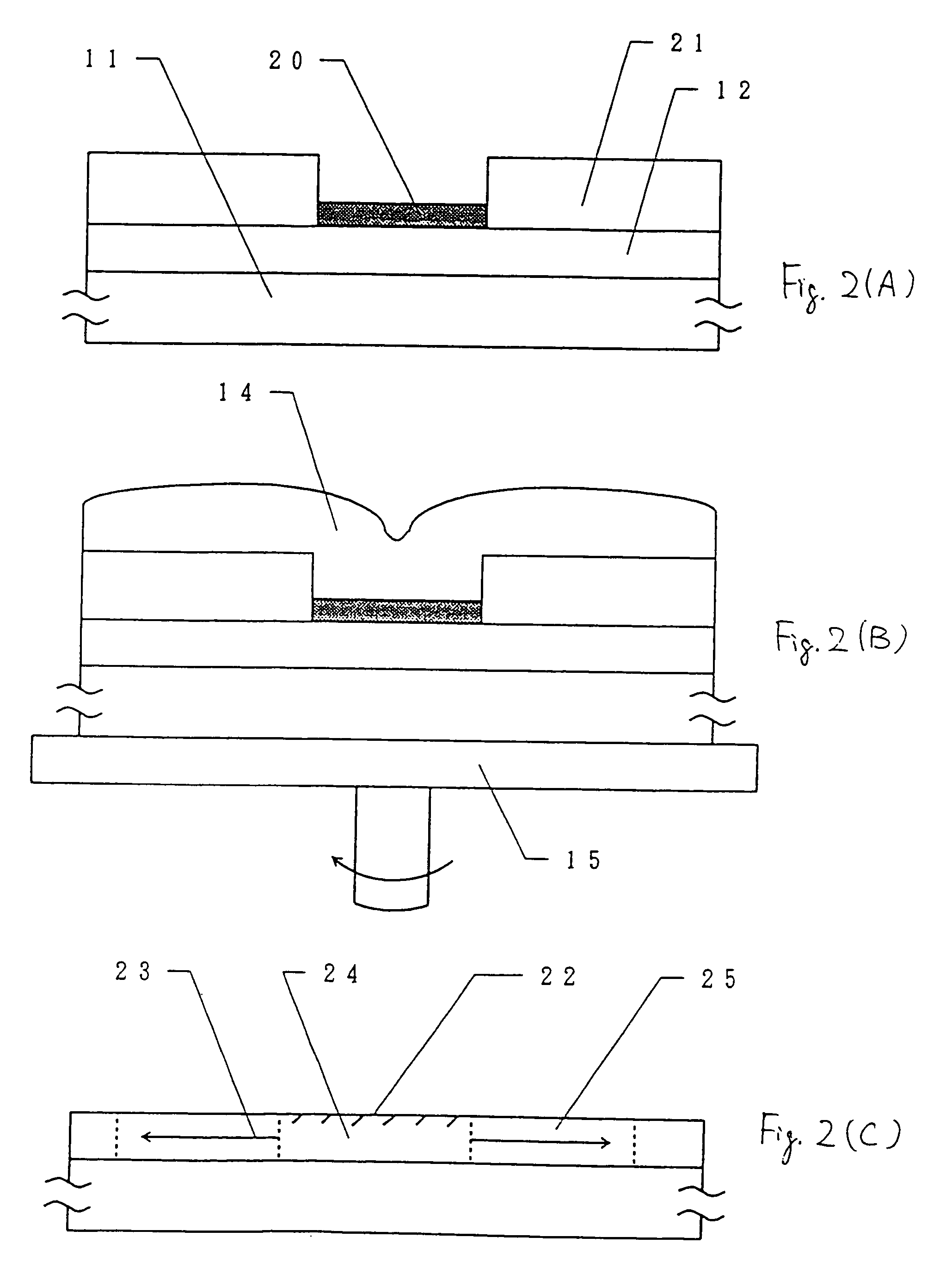
[0093]A manufacturing method of this embodiment is different from Embodiment 1 in that a 1,200-Å-thick silicon oxide film is selectively formed and nickel is selectively introduced by using the silicon oxide film as a mask. Crystal growth is effected parallel with the substrate.

[0094]FIGS. 2(A) to 2(C) schematically shows a manufacturing process according to this embodiment. First, a silicon oxide film 21 having a thickness of more than 1,000 Å, of 1,200 Å in this embodiment, that is to become a mask is formed over a glass substrate 11 (Corning 7059, 10 cm×10 cm). Experiments by the inventors have proved that there occurs no problem even if the silicon oxide film 21 is thinner than 500 Å. It appears that the silicon oxide film 21 can further be thinned if it is dense.

[0095]The silicon oxide film 21 is then shaped into a desired pattern by ordinary photolithography patterning. And a thin silicon oxide film 20 is formed by 5-minute irradiation with ultraviolet light in an ...

Example

Embodiment 3

[0106]This embodiment is directed to the case of forming a TFT by using a crystalline silicon film that is formed by the method of the invention. The TFT of this embodiment can be used in a driver circuit and a pixel area of an active matrix type liquid crystal display device. It goes without saying that the TFT can be applied to not only liquid crystal display devices but also generally called thin-film integrated circuits.

[0107]FIGS. 3(A) to 3(E) schematically show a manufacturing process according to this embodiment. First, a 2,000-Å-thick undercoat silicon oxide film (not shown) is deposited on a glass substrate 11 to prevent impurity diffusion from the glass substrate 11.

[0108]A 500-Å-thick amorphous silicon film is then formed in the same manner as in Embodiment 1. After a hydrofluoric acid treatment for removing a natural oxide film, a thin oxide film of about 20 Å in thickness is formed by irradiation with ultraviolet light in an oxygen atmosphere. Alternatively,...


PUM

PropertyMeasurementUnit
Crystallinityaaaaaaaaaa
Semiconductor propertiesaaaaaaaaaa

Abstract

A very thin oxide film is formed on an amorphous silicon film that is formed on a glass substrate, and an aqueous solution such as an acetate solution added with a catalyst element such as nickel by 10 to 200 ppm (adjustment needed) is dropped thereon. After the structure is held in this state for a predetermined period, spin drying is performed by using a spinner. A crystalline silicon film is obtained by subjecting the structure to a heat treatment of 550° C. and 4 hours and then to laser light irradiation. A crystalline silicon film having a smaller defect concentration is obtained by further performing a heat treatment of 550° C. and 4 hours.

Description

[0001]This application is a continuation of prior application Ser. No. 08 / 781,920, filed Dec. 30, 1996, now abandoned, which is a continuation of application Ser. No. 08 / 519,420, filed Aug. 25, 1995, now abandoned.FIELD OF THE INVENTION[0002]The present invention relates to a semiconductor device using a crystalline semiconductor and a manufacturing method for the same.BACKGROUND OF THE INVENTION[0003]There are known thin film transistors (TFTs), which use a thin film semiconductor that is formed on a substrate. While TFTs are used for various integrated circuits, they attract much attention particularly as switching elements provided for each pixel of an electro-optical device, particularly an active matrix type liquid crystal display device and as driver elements formed in its peripheral circuit portion.[0004]Although an amorphous silicon film is conveniently used for the TFTs, it has a problem of low-grade electrical characteristics. The characteristics of the TFT can be improved...

Claims


Application Information

Patent Timeline
IPC IPC(8): H01L21/3213B05D3/06H01L21/428H01L21/477H01L21/20C23C10/02C23C26/00C23C26/02H01L21/02H01L21/268H01L21/336H01L27/12H01L29/786
CPCC23C10/02C23C26/00H01L21/2026H01L21/2022C23C26/02H01L21/02686H01L21/02422H01L21/02488H01L21/02598H01L21/02532H01L21/02672H01L21/02691H01L21/02675
Inventor FUKUNAGA, TAKESHIOHTANI, HISASHIMIYANAGA, AKIHARU
Owner SEMICON ENERGY LAB CO LTD
Why Eureka
Try Eureka