Method of manufacturing a semiconductor device

a manufacturing method and semiconductor technology, applied in semiconductor devices, semiconductor/solid-state device details, electrical devices, etc., can solve problems such as inability to achieve easy, and achieve the effect of preventing substrate erosion and removing contaminating impurities

Inactive Publication Date: 2008-07-22
SEMICON ENERGY LAB CO LTD
View PDF33 Cites 83 Cited by
  • Summary
  • Abstract
  • Description
  • Claims
  • Application Information

AI Technical Summary

Benefits of technology

[0024]In cases where a glass substrate is used as the substrate and the film surface is etched by immersing the substrate in an acidic solution containing fluorine (such as hydrofluoric acid, dilute hydrofluoric acid), although slight, the glass substrate will erode, and contaminating impurities within the glass substrate mix into the acidic solution, contaminating the acidic solution. If the surface of the films structuring the TFT contacts the contaminated acidic solution, then this is a source of contamination, and is a problem. Then for cases in which a glass substrate is used, in the present invention, the etching is not performed by immersion in the acidic solution, but instead removal of the contaminating impurity in the film surface is performed by using a means of spinning the substrate using a spinning apparatus (spin etcher) and scattering the acidic solution contacting the film surface (also called spin etching, and spin etch). If spin etching is used, then etching can be performed without the contaminated acidic solution contacting the surface of the films structuring the TFT. Note that it is not always necessary to use spin etching. For example, by using a means in which the etching solution flows in a constant direction, it is possible to remove the contaminating impurity in the film surface without contaminating the film surface. Further, by covering the entire top, bottom, and side surfaces of the glass substrate with a film having acid resistance, then it is possible to prevent erosion of the substrate by the acidic solution, and it is also possible to prevent the acidic solution from being contaminated by contaminating impurities within the substrate.

Problems solved by technology

However, successive film deposition must be performed using a successive film deposition apparatus, and cannot be done easily.
In practice, if an insulating film exists on an amorphous semiconductor film, crystallization of the amorphous semiconductor film by annealing is difficult, and therefore crystallization is performed in a state in which there is no insulating film on the semiconductor film.

Method used


Image

  • Method of manufacturing a semiconductor device
  • Method of manufacturing a semiconductor device
  • Method of manufacturing a semiconductor device

Examples


embodiment 1

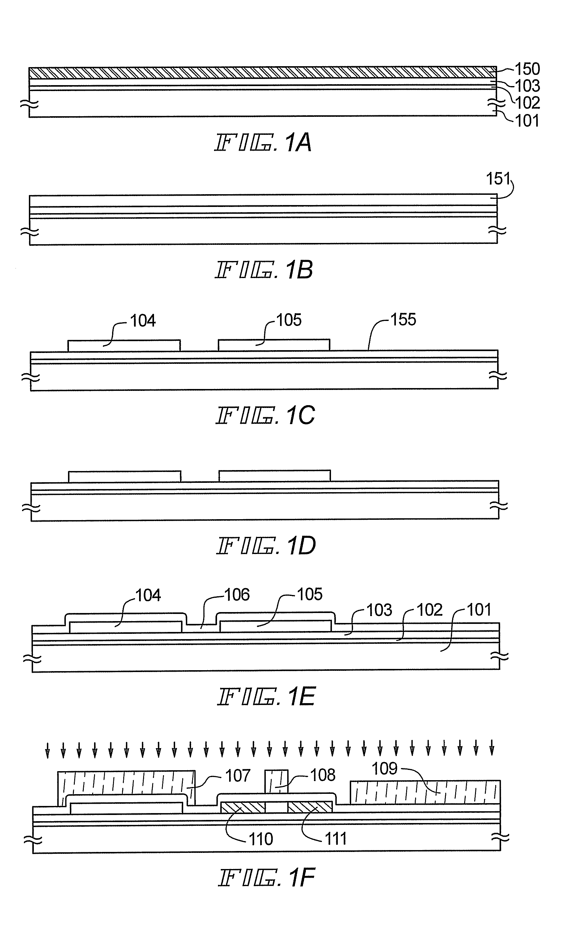
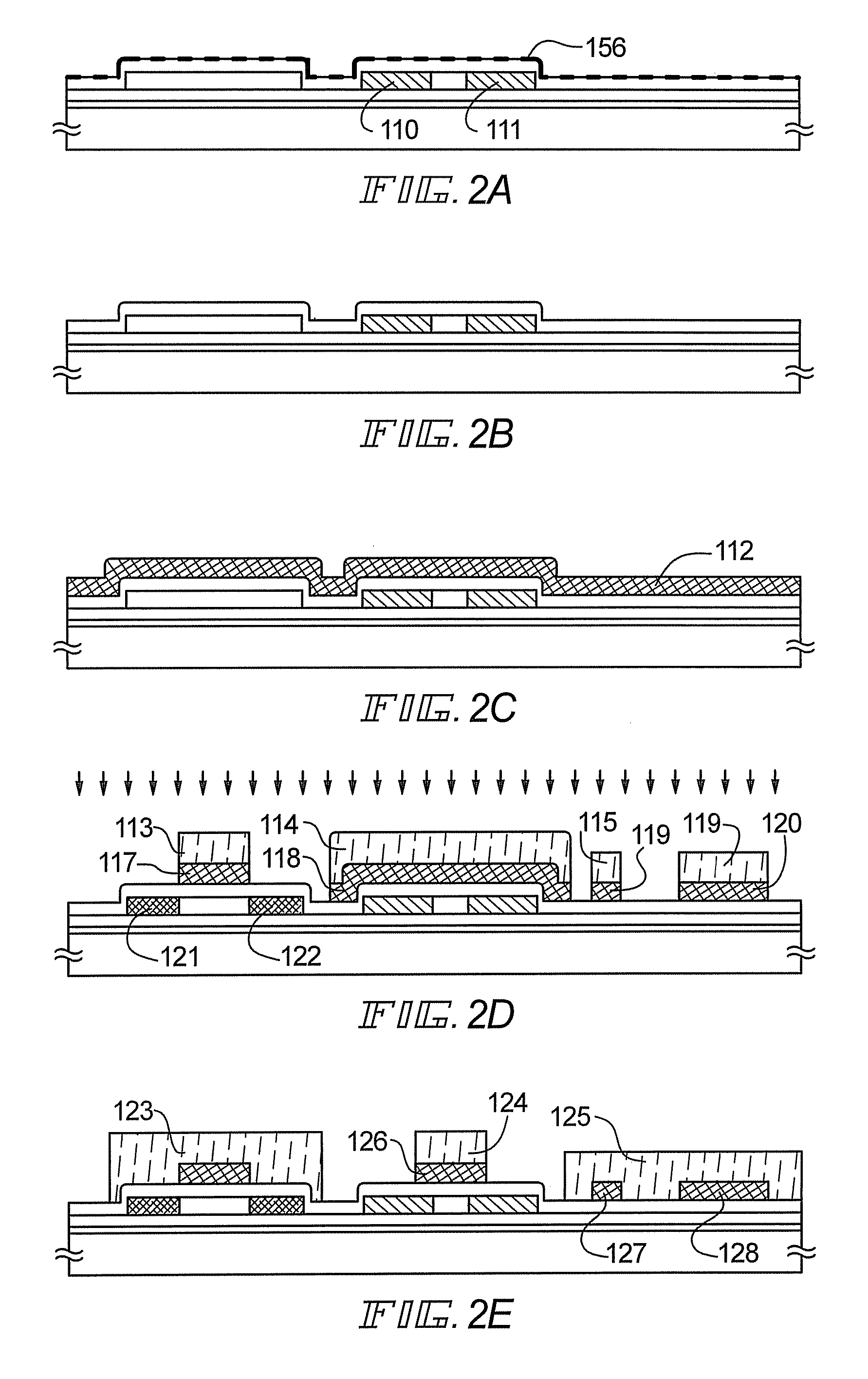
[0045]Embodiment 1 of the present invention is explained by using FIGS. 1A to 3C. An n-channel TFT and a p-channel TFT are manufactured on the same substrate, and an embodiment in which an inverter circuit, a basic CMOS structure, is formed is explained here.

[0046]Substrates such as a glass substrate, a plastic substrate, and a ceramic substrate can be used as a substrate 101. Further, a silicon substrate on whose surface an insulating film such as a silicon oxide film or a silicon nitride film is formed, and a metallic substrate, typically stainless steel, may also be used. Of course it is also possible to use a quartz substrate.

[0047]A base film 102 made from a silicon nitride film, and a base film 103 made from a silicon oxide film are then formed on at least the surface of the substrate 101 on which the TFTs are formed. The base films are formed by plasma CVD or sputtering, and are formed as blocking films in order to prevent diffusion of contaminating impurities which are harmf...

embodiment 2

[0088]Embodiment 2 of the present invention is explained using FIGS. 8A to 9D. An embodiment of the formation of a bottom gate type TFT having an n-channel TFT and a p-channel TFT is explained here.

[0089]First, a glass substrate (Corning 1737, softening point 667° C.) is prepared as a substrate 801. A nitrated silicon oxide film 850 is then formed with a film thickness of 100 to 300 nm as a base film in order to increase the TFT electrical characteristics by preventing diffusion of contaminating impurities from the substrate.

[0090]An example is shown here in which the nitrated silicon oxide film is formed on only one face of the substrate, but it is effective to form the film on both surfaces of the substrate, not only one. By forming the base film on both substrate surfaces, diffusion of contaminating impurities such as sodium from the substrate at the time of manufacture of a semiconductor device can be completely blocked. In addition, it is even more effective to cover all substr...

embodiment 3

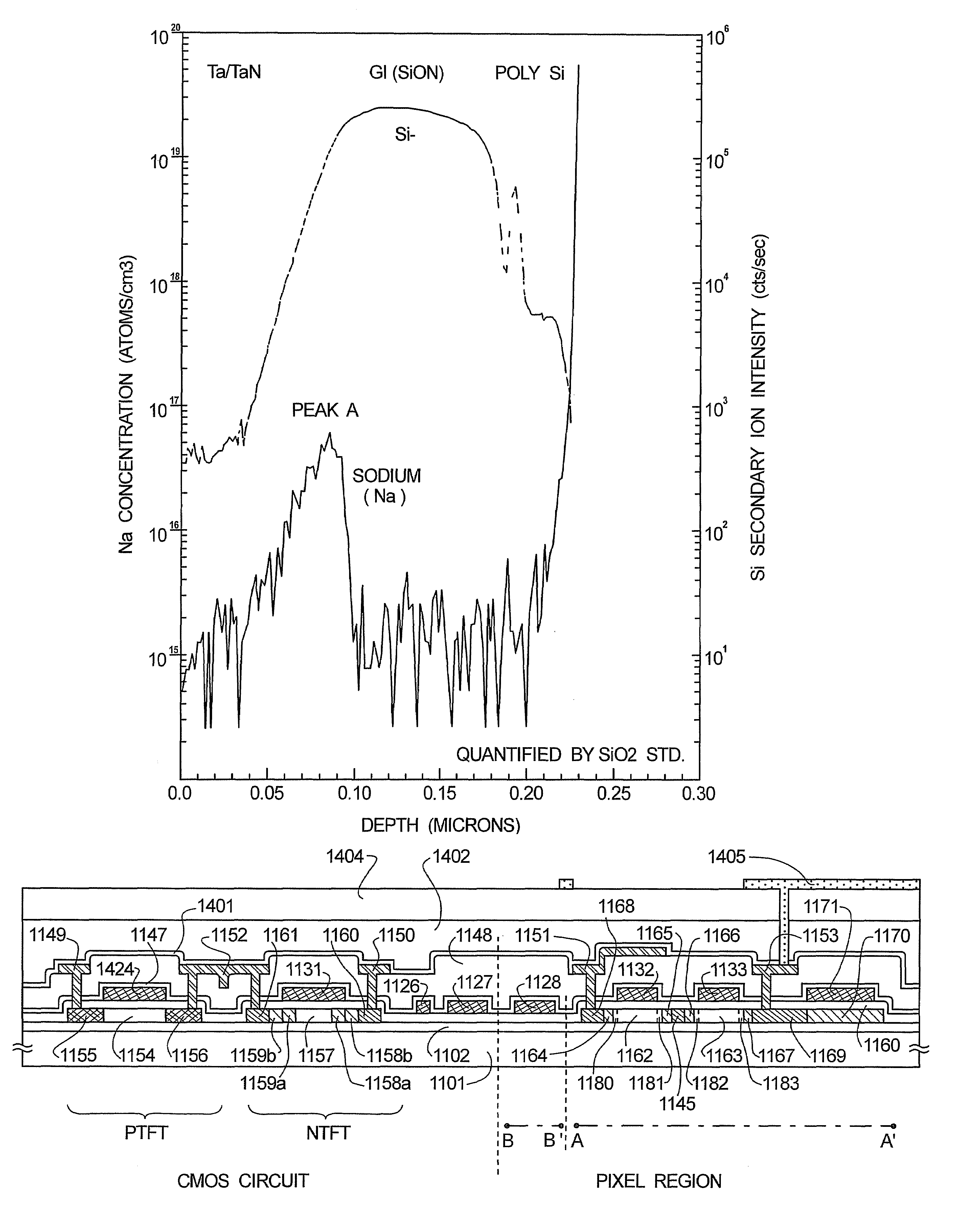
[0106]In Embodiment 3, an example is shown in FIGS. 10 and 11 of a liquid crystal display device equipped with an n-type TFT and a p-type TFT manufactured in accordance with Embodiment 1 above. The semiconductor device of Embodiment 3 is equipped with a circuit in which CMOS circuits and a pixel region are arranged in a matrix state on the same substrate.

[0107]A cross sectional diagram of the semiconductor device of Embodiment 3 is shown in FIG. 10. In consideration of reliability, the TFTs are formed over a base film 1102 formed on a substrate 1101 in Embodiment 3.

[0108]The CMOS circuit shown in the left side of FIG. 10 is called an inverter circuit, and is a basic circuit structuring the semiconductor circuit. By combining these types of inverter circuits, a more complex logic circuit structure can be made.

[0109]The p-channel TFT of the CMOS circuit is formed with a channel forming region 1154, and third valence electron control impurity regions 1155 and 1156. Boron is doped at a ...


PUM


Abstract

A reduction in contaminating impurities in a TFT, and a TFT which is reliable, is obtained in a semiconductor device which uses the TFT. By removing contaminating impurities residing in a film interface of the TFT using a solution containing fluorine, a reliable TFT can be obtained.

Description

BACKGROUND OF THE INVENTION[0001]1. Field of the Invention[0002]The present invention relates to a semiconductor device, such as a thin film transistor (TFT), using a crystalline semiconductor film formed over a substrate, and to a method of manufacturing the same. The semiconductor device of the present invention includes not only elements such as a thin film transistor (TFT) or a MOS transistor, but also includes liquid crystal display devices, EL display devices, EC display devices, and image sensors having a semiconductor circuit (such as a microprocessor, a signal processing circuit, or a high frequency circuit) structured by these insulating gate type transistors. In addition, the semiconductor device of the present invention includes electronic equipment which is loaded with these display devices, such as a video camera, a digital camera, a projector, a goggle display, a car navigation system, a personal computer, or a portable information terminal.[0003]2. Description of the...

Claims


Application Information

Patent Timeline
Patent Type & Authority Patents(United States)
IPC IPC(8): H01L21/00H01L21/84
CPCH01L27/1214H01L29/66757H01L29/66765H01L27/127H01L29/78621H01L27/1222H01L2924/0002H01L23/10H01L2924/00H01L27/1248H01L27/1274H01L27/1288H10K50/844H10K50/846H10K59/124
Inventor KADONO, MASAYAYAMAZAKI, SHUNPEIYAMAUCHI, YUKIOKITAKADO, HIDEHITO
Owner SEMICON ENERGY LAB CO LTD
Why Eureka
Try Eureka