Insulated gate field effect semiconductor devices and method of manufacturing the same

a semiconductor device and field effect technology, applied in non-linear optics, instruments, optics, etc., can solve the problems of short channel effect, high operational speed, and gives rise to other problems, and achieve low on-state resistance and high switching speed

Inactive Publication Date: 2008-11-25
SEMICON ENERGY LAB CO LTD
View PDF151 Cites 11 Cited by
  • Summary
  • Abstract
  • Description
  • Claims
  • Application Information

AI Technical Summary

Benefits of technology

[0016]It is an object of the present invention to provide a method of manufacturing an insulated gate field effect semiconductor device within a small area which has a high switching speed and a low on-state resistance.
[0024]It is, however, not so difficult in accordance with the present invention to control the relationship. The spread of the dopant within the lightly doped regions 103 due to secondary scattering of the ion implantation can be controlled by adjusting the acceleration energy of ions. The shrinkage of the conductive film 101 due to the anodic oxidation is also controlled by adjusting the thickness of the oxide film, i.e. by adjusting the oxidation condition. The thickness of the oxide film 104 can be controlled within ±10 nm from a target thickness. The secondary scattering can be controlled at the same order accuracy. Namely, by accurately designing the respective dimensions, the optimum relationship between the lightly doped regions 103 and the gate electrode 105 can be achieved only with an error as small as 10 nm.
[0031]Another assumption is based upon difference between the noncrystal and the crystal in band-gap. FIG. 4(B) illustrates the energy band structure of a semiconductor device with a LDD structure when no gate signal is supplied. FIG. 4(C) illustrates the energy band structure of a semiconductor device with a LDD structure when a large gate voltage is supplied in the reverse direction. In this case, small carrier leakage takes place through the device due to tunnel effects and hopping among trapping levels existing in the band-gap. The provision of the LDD structure is effective to increase the band-gap at the junctions so that the carrier leakage is suppressed as compared with a device having no LDD structure. The improvement due to the LDD structure is particularly remarkable when the FET is a thin film transistor (TFT) because a TFT utilizes a nonuniform semiconductor material such as polysilicon forming trapping levels therein which are considered to originate from grain boundaries.

Problems solved by technology

This also results in a high operational speed because the short channel length decreases the time required for carriers to pass across the channel.
The miniaturizing, on the other hand, gives rise to other problems, i.e. short channel effects.
One of the most serious problems thereof is hot electron effects.
As a result, the characteristics of the device are unstable.
The problems associated with the short channel designs, however, are not completely solved by this technique.
Another problem is the resistance of the gate electrode which has become narrow.
Even if the switching speed of the device is increased by the short channel, the speed-up may possibly come to naught due to propagation delay along the high resistant gate electrode.
These techniques, however, can not solve the high resistance problem when the width of the gate electrode is no larger than 0.3 micrometer.
The increase of double the source and drain resistance, however, cancels the improvement.
In addition to this, the width of the spacer has been substantially dispersed, due to expected variations of production, which results in dispersed characteristics of the products.
The conventional LDD technique has brought high integrations and high speeds and, on the contrary, impeded further improvement.

Method used


Image

  • Insulated gate field effect semiconductor devices and method of manufacturing the same
  • Insulated gate field effect semiconductor devices and method of manufacturing the same
  • Insulated gate field effect semiconductor devices and method of manufacturing the same

Examples


first embodiment

[0046]Referring now to FIGS. 3(A) to 3(D), a method of manufacturing an n-channel thin film field effect transistor in accordance with the present invention will be explained.

[0047]A low temperature oxide film 302 is deposited on a quartz substrate 301 by low pressure CVD to a thickness of 10 to 500 nm, for example, 100 nm as illustrated in FIG. 3(A). An intrinsic amorphous silicon semiconductor film is deposited in the same manner over the oxide film 302 by low pressure CVD to a thickness of 10 to 100 nm, for example, 20 nm. Alternatively, by elevating the deposition temperature, the semiconductor film is deposited in a microcrystalline or polycrystalline phase instead of the amorphous phase. The amorphous semiconductor film may be deposited by plasma CVD or photo-CVD instead of low pressure CVD. A rectangular active region of 10 micrometers×30 micrometers is separated from the amorphous film by patterning and exposed to laser light emitted from a KrF excimer laser in order to crys...

second embodiment

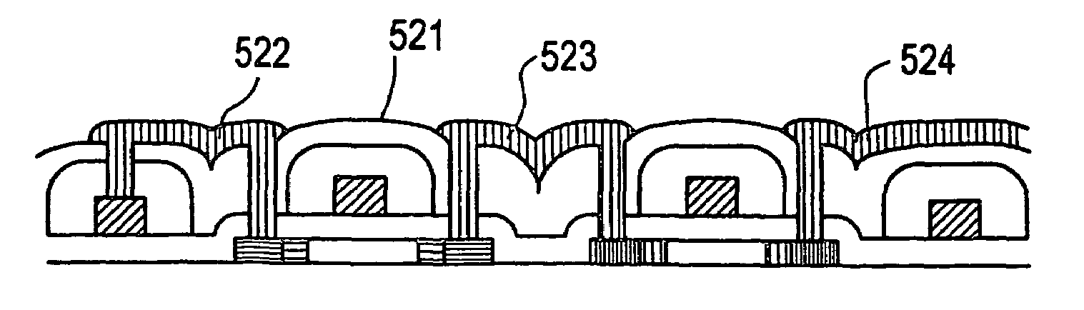
[0053]Referring now to FIGS. 5(A) to 5(E), FIGS. 6(A) to 6(C) and FIGS. 7(A) to 7(C), initially to FIGS. 5(A) to 5(E), a method of manufacturing complementary thin film field effect transistors in accordance with the present invention will be explained.

[0054]An intrinsic amorphous silicon semiconductor film is deposited on a substrate of Corning 7059 glass substrate to a thickness of 150 nm by plasma CVD and crystallized in nitrogen at 600° C. for 60 hours. A pair of island-shaped rectangular active regions 502 and 503 are separated from the amorphous film by patterning.

[0055]A silicon oxide film is then deposited on the substrate 501 over the active regions to a thickness of 115 nm by sputtering. An aluminum film is next deposited on the oxide film to a thickness of 100 to 800 nm, for example, 500 nm by electron beam vacuum evaporation. The aluminum film is patterned to form aluminum patterns 506 and 507 of 8 micrometers width (in the left to right direction) to be a gate electrode...

third embodiment

[0062]Referring next to FIGS. 8(A) to 8(D), a method of manufacturing a thin film field effect transistor in accordance with the present invention will be explained.

[0063]A silicon oxide film 802 is deposited on a substrate 801 of Corning 7059 glass to a thickness of 100 nm by sputtering. An intrinsic amorphous silicon semiconductor film is then deposited on the oxide film 802 to a thickness of 50 nm by plasma CVD. Another silicon oxide film 804 is further deposited on the semiconductor film to a thickness of 20 nm by sputtering for the purpose of protection of the semiconductor film. The semiconductor film is then crystallized by thermal annealing in nitrogen at 600° C. for 72 hours. These semiconductor film and the silicon oxide film are partially removed to leave an island-shaped rectangular active region of 30 micrometers length in the left-right direction and 20 micrometers width normal to the drawing sheet as denoted by numerals 803 followed by removing the protective oxide fi...


PUM

PropertyMeasurementUnit
lengthaaaaaaaaaa
lengthaaaaaaaaaa
widthaaaaaaaaaa

Abstract

An LDD structure is manufactured to have a desired aspect ratio of the height to the width of a gate electrode. The gate electrode is first deposited on a semiconductor substrate followed by ion implantation with the gate electrode as a mask to form a pair of impurity regions. The gate electrode is then anodic oxidized to form an oxide film enclosing the electrode. With the oxide film as a mask, highly doped regions are formed by ion implantation in order to define lightly doped regions between the highly doped regions and the channel region located therebetween.

Description

BACKGROUND OF THE INVENTION[0001]1. Field of the Invention[0002]The present invention relates in general to an insulated gate field effect semiconductor device and method of manufacturing the same.[0003]2. Description of the Prior Art[0004]A variety of approaches have been carried out in order to miniaturize integrated circuits and achieve a higher packing density in a chip. Particularly, remarkable advances have been reported in the development of the technology to miniaturize insulated gate field effect semiconductor devices, denoted as MOSFET for short. MOS is the acronym of Metal Oxide Semiconductor. The metal used in MOSFETs generally includes, in addition to genuine metals, conductive materials such as semiconductors having a sufficient conductivity, alloys composed of semiconductor(s) and / or metal(s). The oxide generally includes, in addition to genuine oxides, insulating materials having a sufficient resistivity such as nitrides. Although these materials do exactly not corre...

Claims


Application Information

Patent Timeline
Patent Type & Authority Patents(United States)
IPC IPC(8): H01L29/04H01L29/78G02F1/1362H01L21/265H01L21/336H01L21/60H01L21/77H01L21/84H01L27/12H01L29/49H01L29/786
CPCH01L21/76897H01L27/1214H01L29/04H01L29/78675H01L29/66757H01L29/78621H01L29/78627H01L29/78651H01L29/78666H01L29/4908G02F1/13454G02F2001/136245G02F1/136245H01L27/127
Inventor YAMAZAKI, SHUNPEITAKEMURA, YASUHIKOZHANG, HONGYONG
Owner SEMICON ENERGY LAB CO LTD
Why Eureka
Try Eureka