
Material for purification of semiconductor polishing slurry, module for purification of semiconductor polishing slurry and process for producing semiconductor polishing slurry

a technology for purifying slurry and polishing wafers, which is applied in the direction of manufacturing tools, separation processes, lapping machines, etc., can solve the problems of contaminated polished wafers, step coverage, change in film thickness, etc., and achieve the effect of improving the level of removal of metal ions

Inactive Publication Date: 2009-12-01
NOMURA MICRO SCI CO LTD
View PDF7 Cites 6 Cited by
  • Summary
  • Abstract
  • Description
  • Claims
  • Application Information

AI Technical Summary

Benefits of technology

The present invention provides a material for purification of a semiconductor polishing slurry that has a functional group capable of forming a metal chelate fixed onto at least the surface of a fibrous substrate. This material can be used to remove metals that are present in the slurry as impurities. The substrate has a fibrous form, which allows for filtering out the impurities by passing the slurry through a column. The material can be used alone or in a mixed form. The substrate can be made of various fibers such as cellulose, polyvinyl alcohol, polyethylenimine, polyester, polyvinyl chloride, polyacrylonitrile, polyamide, polyolefine, and nonwoven fabric. The substrate should have an ethylenical hydroxyl group and a hydroxyl value of 40 mgKOH / g or more for optimal performance. The use of this material can improve the purity of the semiconductor polishing slurry.

Problems solved by technology

If a step portion because of the unevenness becomes large, there is a possibility of various failures such as degradation in coverage (step coverage) on step portions when forming a film, a change in film thickness of the photoresist on the step portions in a lithography process, and the like.
Hei 11-186201, for example, when a silicon wafer or the like is polished with a semiconductor polishing slurry containing such impurity metal ions and the like, there is a problem that the polished wafer is contaminated by the impurity metal ions because copper, iron and nickel ions are particularly easy to spread in silicon.
This method has an advantage that the metal ions can be removed relatively easily, but because the ion-exchange group is a sulfonic acid group (sulfonyl group) or a carboxylic acid group (carboxyl group), it has a high pH dependency and very poor metal ion adsorption selectivity.
Therefore, if there are alkali metal ion such as sodium ion or potassium ions, the ion-exchange resin has a disadvantage that the removal efficiency of other metal ions subject to the removal drops considerably.
And, when the ion-exchange resin is used to purify the semiconductor polishing slurry, there is a problem that the polishing performance is largely affected because the pH of the purified polishing slurry changes depending on a type of the functional group fixed onto the resin.
However, the chelate resin has a bead-like or particle-like shape which has a chelate functional group introduced into a polymer, such as styrene-divinylbenzene, which has a low polarity and a rigid three-dimensional crosslinked structure, and has a problem that a capturing rate of metal ions is low because a rate of diffusion into the bead-like or partile-like chelate resin required for selective separation of a very small amount of metals is slow.
That is the semiconductor polishing slurry contains a high concentration of a polishing material and a pH adjuster up to several percent, so that the chelate resin developed in order to perform selective separation in a general water system is quite hard to remove by selectively separating a very small amount of ionic metals, colloidal metals or hydroxide metals from the semiconductor polishing slurry.

Method used


Image

  • Material for purification of semiconductor polishing slurry, module for purification of semiconductor polishing slurry and process for producing semiconductor polishing slurry
  • Material for purification of semiconductor polishing slurry, module for purification of semiconductor polishing slurry and process for producing semiconductor polishing slurry
  • Material for purification of semiconductor polishing slurry, module for purification of semiconductor polishing slurry and process for producing semiconductor polishing slurry

Examples


examples

[0077]The present invention will be described more specifically with reference to examples. It is to be understood that the present invention is not limited to the examples, and various modifications can be made without deviating from the spirit and scope of the invention.

examples 1 through 7

Material for Purification of Polishing Slurry in the Production of a Semiconductor Silicon Wafer and Ability of Removing Metals Contained in the Polishing Slurry

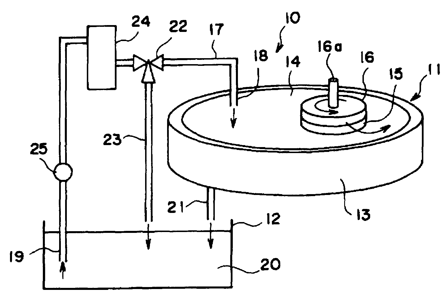
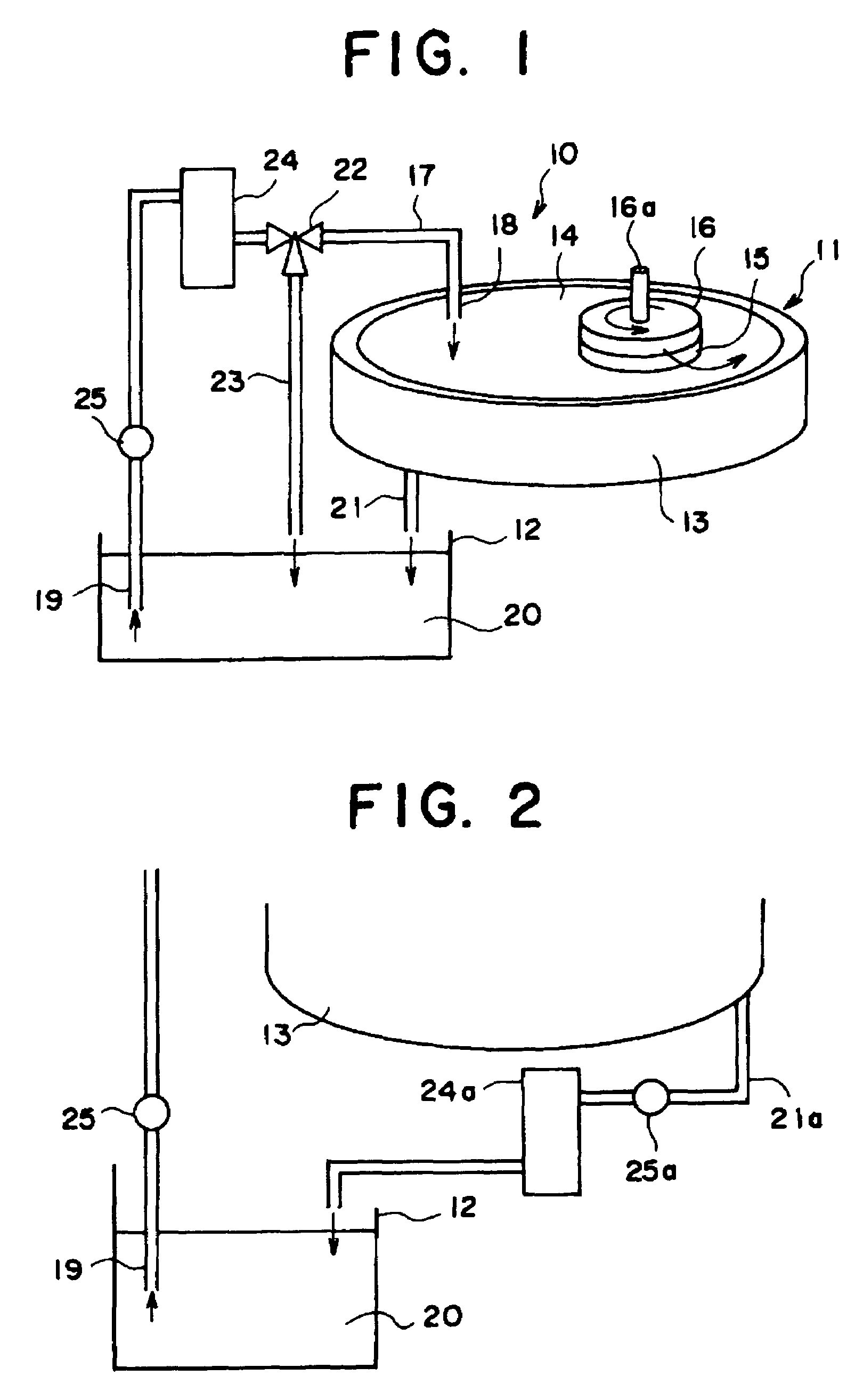
[0078]The slurry 20 having 3 wt % of a colloidal silica stock solution simulating the polishing slurry diluted to ten times with ultrapure water was accumulated in the polishing slurry tank 12 of the apparatus shown in FIG. 1. As to the metal impurity concentrations of the slurry, iron, copper and nickel, which were big obstacles contaminating the silicon wafer, were 0.01 ppb, respectively.

[0079]Iron, copper and nickel were added so to become 30 ppb to 50 ppb in the slurry 20 with contamination by the production apparatus and environment taken into consideration and thoroughly stirred to uniformly disperse in the slurry 20.

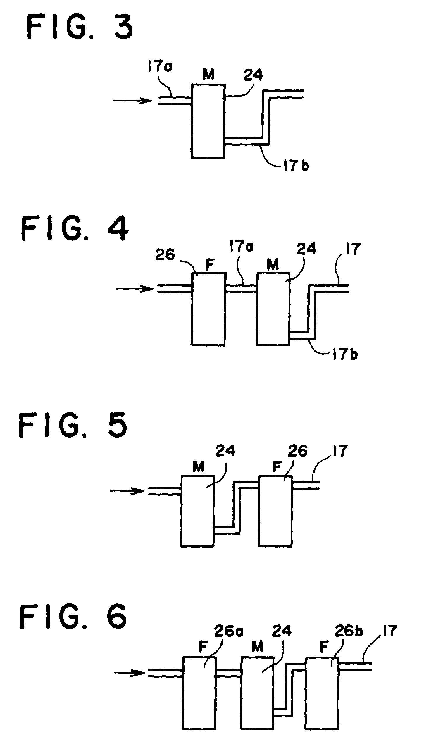
[0080]Meanwhile, the metal removing devices 24 in which the various types of chelate fiber shown in Table 1 were filled respectively were connected in parallel in the midpoint of the polishing slurry feedi...

examples 8 through 12

Material for Purification of Polishing Slurry and Removability of Metals in Polishing Slurry in CMP Process for Production of Semiconductor Device

[0102]In a process of producing a device on an Si wafer by the apparatus shown in FIG. 1, the CMP process was conducted to polish metal wiring which is comprised of copper, tungsten and the like. The polishing slurry tank 12 had a polishing slurry amount of 50 liters, a copper and tungsten concentration before polishing was 1 ppm or less, and 60 ppm of iron was added as a polishing aid. In the polishing slurry used for polishing without charging the chelate fiber in the metal removing device 24, the concentrations of tungsten and copper were increased to 200 ppm and 12 ppm respectively, and pH was acid of 2.3.

[0103]Then, the metal removing device 24 was filled with various types of polishing slurry purifying materials 47, and the three-way valve 22 which was disposed at the midpoint of the polishing slurry feeding pipe 17 was used for each...


PUM

PropertyMeasurementUnit
hydroxyl valueaaaaaaaaaa
lengthaaaaaaaaaa
lengthaaaaaaaaaa

Abstract

A material for purification of a semiconductor polishing slurry that without changing of pH value, is capable of efficiently purifying a polishing slurry to thereby not only prevent metal contamination of a polished object as effectively as possible but also achieve recycling of a polishing slurry without any problem; a relevant module for purification of a semiconductor polishing slurry; and a process for purifying a semiconductor polishing slurry with the use thereof. In particular, a material for purification of a semiconductor polishing slurry characterized in that it comprises a fibrous substrate having a functional group capable of forming a metal chelate or such a functional group together with hydroxyl fixed onto at least the surface thereof. This material for purification of a semiconductor polishing slurry is, for example, used in such a manner that it is inserted in a container fitted with polishing slurry inflow port and outflow port while ensuring passage of polishing slurry flow.

Description

TECHNICAL FIELD[0001]The present invention relates to a material for purification of a semiconductor polishing slurry, which has a functional group capable of forming chelate with metal ions, for example, metals such as iron, aluminum, copper, nickel, zinc, chromium, manganese and tungsten, contained in a polishing slurry (semiconductor polishing slurry) used in a semiconductor production process, or a material has a functional group capable of forming chelate with the above metals and a hydroxyl group fixed onto a fibrous substrate; a module for purification of a semiconductor polishing slurry; and a process for purification of a semiconductor polishing slurry using them.[0002]In the case of this field, the semiconductor production includes at least a process of producing base materials such as wafers, glass for liquid crystals and masks, members of a production device, and a device producing process for producing elements and patterns by fabricating the above materials.BACKGROUND ...

Claims


Application Information

Patent Timeline
Patent Type & Authority Patents(United States)
IPC IPC(8): B24B7/22B01J45/00B01J47/04B01J47/10B01J47/12B01J47/14B24B37/00B24B57/02C02F11/00C23F1/46H01L21/304
CPCB01J45/00B01J47/123C23F1/46B24B57/02B24B37/00B01J47/127H01L21/304
Inventor ABE, MITSUGUNAMBU, NOBUYOSHIITO, OSAMUOGITSU, MASAAKIINOMATA, KAZUO
Owner NOMURA MICRO SCI CO LTD
Learn More